Fraunhofer Institute for Reliability and Microintegration IZM
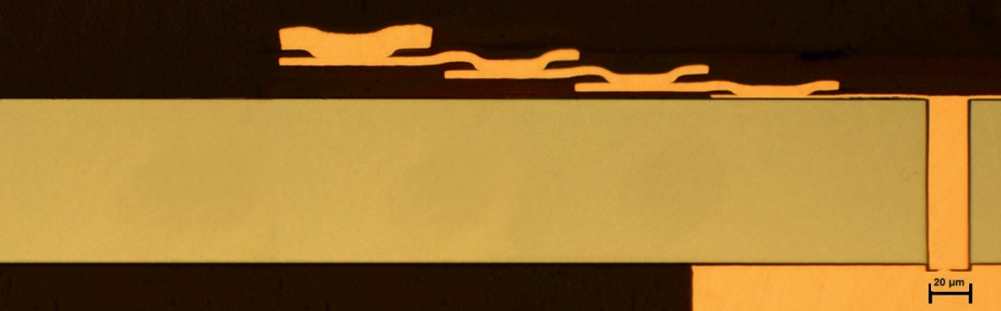
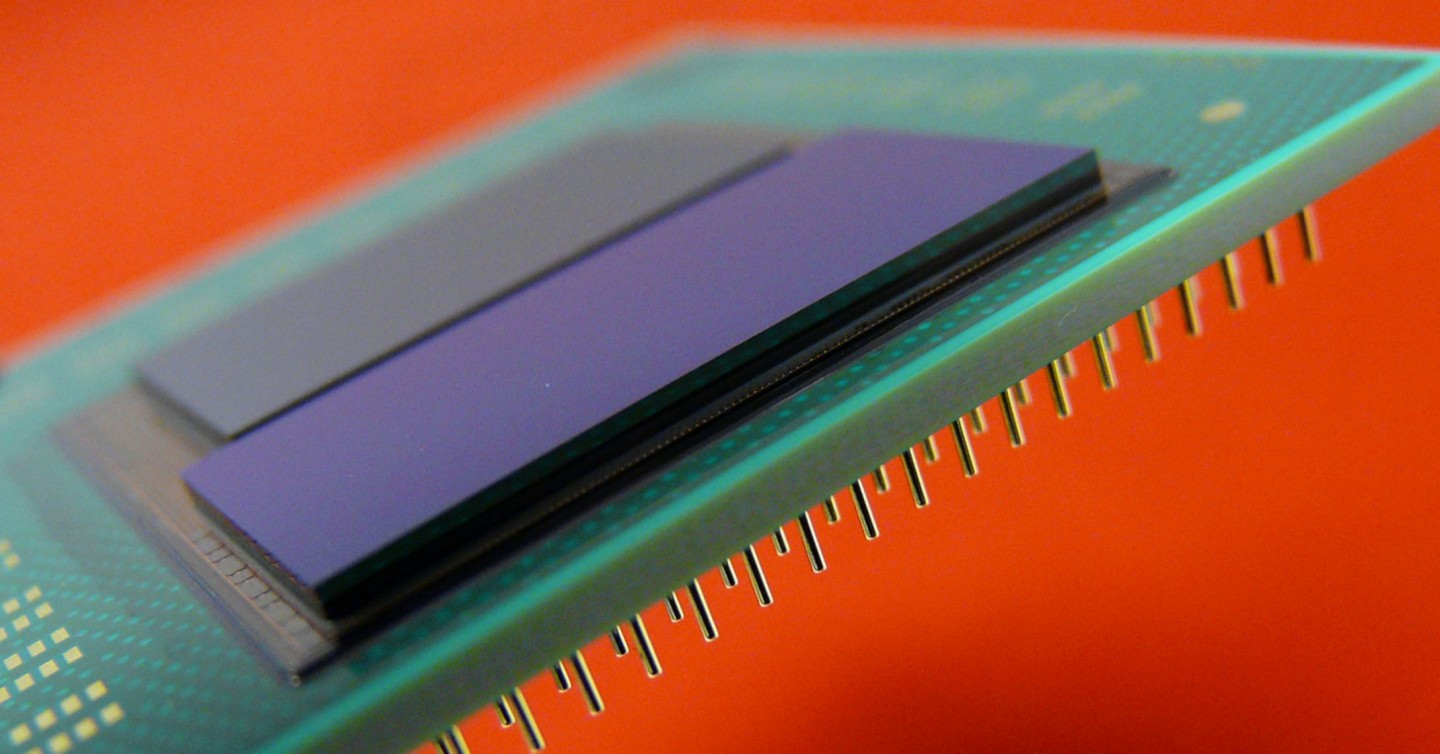
3D system integration is one of the most important topics in current packaging and interconnection. Based on the vertical stacking of system components the concept offers specific advantages with regard to the heterogeneous integration of different components, such as sensors, processors, memories or antennas.
The use of the third dimension not only allows for more compact packaging, but also for shorter electrical interconnects, which in turn makes the entire system more powerful and efficient.
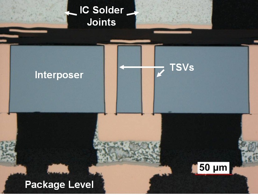
Current projects are focused on vertical integration of systems based on logic- and memory- or sensor chips as well as transceivers and antennas. Therefore through silicon vias (TSVs) are created into the devices at wafer scale to enable vertical routing of electrical signals from their top to their bottom side as well as subsequent vertical stacking.
The established TSV middle or TSV last processes comprise via formation by dry etching, via isolation, via metallization by copper filling, high density multi layer wiring, wafer thinning as well as handling and processing of ultra thin wafers.
The same technology is used to create silicon interposers with vertical through contacts as well as which act as component carriers or adapters between integrated circuits with highest IO densities and organic carriers.