Fraunhofer Institute for Reliability and Microintegration IZM
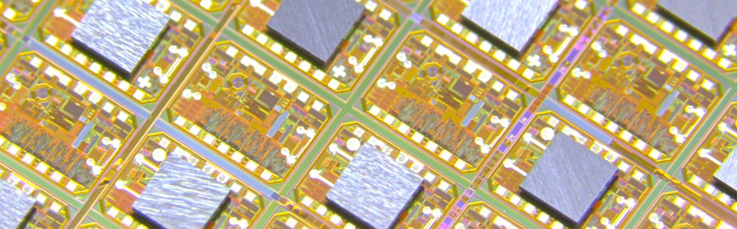
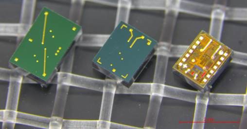
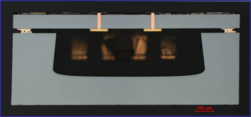
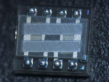
The combination of active or passive TSV silicon interposer wafers with cap wafers by wafer to wafer bonding technologies offers new possibilities for hermetic wafer level packaging of MEMS components. Based on its 200 mm / 300 mm compatible advanced wafer level packaging process lines, Fraunhofer IZM can support such new hermetic wafer level MEMS packaging concepts.
Process scheme
The process scheme includes TSV formation into passive interposer or active CMOS wafers including wafer thinning and thin wafer processing on temporary carrier wafers for TSV back side reveal and RDL / contact formation at wafer back side. Following, the MEMS are assembled onto the back side of the thin TSV wafer which is done by sequential or collective die to wafer bonding. Additionally, cap wafers are manufactured with recesses and metal bond frames to fit exactly to the corresponding TSV wafers with the mounted MEMS. Finally, the cap wafers are bonded to the TSV wafers using a dedicated soldering regime. With that, all mounted components can be hermetically sealed in inert atmosphere or vacuum.