 Fraunhofer Institute for Reliability and Microintegration IZM
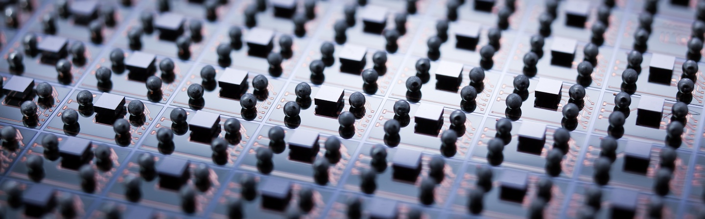
Wafer Level Packaging is a synonym for the whole technology spectrum enabling direct chip attachment on PWB or other substrates by Flip Chip Interconnection. In contrast to pure bumping processes additional thin film wiring layers are required featuring a higher level of integration by embedding active or passive devices onto the chip. The technology is feasible for any kind of CMOS wafers but also for III/V or even sensors.
The basic process is the so called redistribution process based on thin film technology. Thin film polymers like PI, BCB, PBO, Epoxy or other polymers or even thin glass layers are used for the electrical isolation between the layers and the mechanical and electrical decoupling to the base wafer. The metal routings are deposited by a combination of sputtering and electroplating using a photo resist process. Mostly Cu is used with a diffusion barrier and adhesion layer of TiW or pure Ti.
The final metallization can be adapted to the required bonding process for the next level of integration. Solder balls are deposited for standard FC-assembly. The size of the solder balls can be varied from ultra-fine pitch of 20 µm using electroplated bumps to the well established area array pitch of 500 µm using large preformed balls using ball drop. Thick Au (typically 5 – 20 µm) is used for a final metallization if an adhesive joint (ACA, NCA) is required on a board, glass or a flex. The final metallization can also be adapted to wire-bonding interconnection using Au or Al.
The emphasis of Fraunhofer IZM is in a custom-specific development or prototyping. The technology can be adapted to nearly all applications and requirements. Process transfer is an option for production.