Key Research Areas

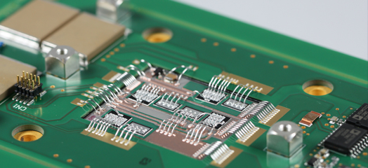
Packaging for power electronics

Besides die attach soldering and Al heavy wire bonding, new packaging concepts are pursued to built power electronics systems which shall provide improved thermal performance and higher reliability. By replacing the wire bond with an area contact on both sides of the chips the thermal performance can be improved.

Silver sintering is one of the new die attach technologies which result in a higher life time of the whole power package. Silver is ductile, it has a high melting point and a very high thermal conductivity. Therefore, especially for a higher performance and higher operating temperatures Ag sinter joints are very promising. There is another new joining technology currently under development which is referred to as “transient liquid phase soldering” or “bonding” (TLPS or TLPB). The idea behind this technology is that the Sn-based solder is transformed in intermetallic phases which have a higher melting temperature than the solder alloy has had before the joining has been carried out. The higher melting point is necessary to withstand higher operating temperatures or for withstanding subsequent soldering processes during manufacturing.

The wire or ribbon bonds may also be improved regarding their life time. Using Cu wire instead of Al reduces the thermal mismatch between the Si die and the wire bond material. In order to be able to use Cu bonds the power chips have to have a Cu metallization on top. The IZM has the capability to deposit Cu layers on semiconductor wafers using electroplating.

Last not least the power package is accomplished by applying an encapsulation material, which can also be done at the Fraunhofer IZM.

IZM-services relating to packaging and interconnection

  • Die-attach for high-temperature applications (Ag sintering and transient liquid phase bonding)
  • Development of alternative technologies like flip-chip, ultrasonic bonding, Cu heavy wire and ribbon bonding, sandwich assemblies (double-sided cooling of chips
  • Ultrasonic welding of load connections
  • Heavy wire bonding (up to 500 µm) of power modules
  • Ribbon laser bonding 
  • Packaging of GaAs, InP, SiC and GaN, as well as thinned semiconductors
  • Encapsulation of power modules
  • Wafer-level packaging of power semiconductors
  • Embedding of power modules


Ag sintering of large areas

Large-area silver sintering between metallized ceramic substrates and a transfer cooler is suitable for achieving the highest possible thermal conductivity while maintaining a long service life.


Power module for Formula 1 with substrate water cooling

Main goals for a Formula 1 power module are highest power density and lowest weight. Volume and weight of presented converter could be reduced by roughly 50 percent compared to previous versions.


Advanced driver by Fraunhofer IZM

Miniaturized, Zero-Dead-Time High-Efficiency Drivers for Si, SiC, and GaN Applications.


Low-inductance packages for fast-switching semiconductors

The secret for miniature converters with high power density.


Compact converters enabling high power density

Due to the low switching losses when using the novel wide band-gap semiconductor generation made from gallium nitride and silicon carbide, respectively, it is possible to increase the switching frequency of power electronic systems significantly.  


Power electronics - from chip to system


Embedding

Miniaturization and packaging of power electronics by embedding of semiconductor switches into the build-up layers of a printed circuit board has experienced a considerable development throughout recent years. Besides commercialization and the introduction of the first products into the market, there are still a number of interesting new concepts under scientific and technological investigation.

Laser microwelding

Laser microwelding based on a fully automatic wire bonder for processing ribbon of copper, aluminium, nickel, gold, silver and platinum with widths up to 2 mm and thicknesses up to 0.5 mm Particularly suitable for vibrating or pressure-sensitive substrates, such as battery contacts. Module size maximum 650 mm × 350 mm, accuracy ≤ ±5 µm, industrial welding monitor for process control. Use of this method also in connection with process development and quality assessment even after mechanical or thermal aging.

Projects

ULTIMO

Ultra-compact, ultra-reliable power module

We are working with automotive manufacturers and suppliers to design and manufacture an ultra-compact power module with double-sided cooling for high power density applications as part of an industry-based research consortium on “Improving energy efficiency using power electronics”, which is funded by the German federal ministry of education and research (BMBF).