News
A milestone in manufacturing technology
Fan-out panel level packaging (PLP) is an extremely cost-efficient manufacturing technology with huge commercial potential. Fraunhofer IZM recently brought together international stakeholders to begin shaping a long-term research strategy, with an expert symposium on June 28-29.
According to the statistics portal Statista, more than 1.4 billion cell phones were sold globally last year. Each new generation of smartphone by leading brands like Apple and Samsung is manufactured in the hundreds of thousands each day. Most of the necessary components, such as memory chips and microprocessors are purchased separately and then assembled into units in assembly plants. This means that when suppliers change the size of components, the processing flow is thrown into disarray. “If a memory chip is suddenly smaller, everything in the assembly process has to be changed,” explains Dr. Michael Töpper, Fraunhofer IZM scientist. But high-pressure manufacturing environments do not allow for constantly reconfiguring an assembly process.
So what to do if a component suddenly doesn’t fit anymore, because the chip is now smaller? Well, the component can be artificially enlarged and cut to size anew. Fan-out wafer level packaging is one means of accomplishing this. Here the individual chips are mounted on a temporary carrier and integrated into a new, reconfigured wafer using a molding process. Once the newly molded wafer with the embedded chips has been detached for the substrate, interconnection can be performed. Here, several chips can be interconnected or the electrical terminal pads can simply be routed to the chip surface that has been enlarged using the molding compound. In this way, extremely flexible yet miniaturized packages and components can be produced. However, the number of components that can be simultaneously processed on the reconfigured wafer is restricted by the latter’s traditional maximum size of 300 mm.
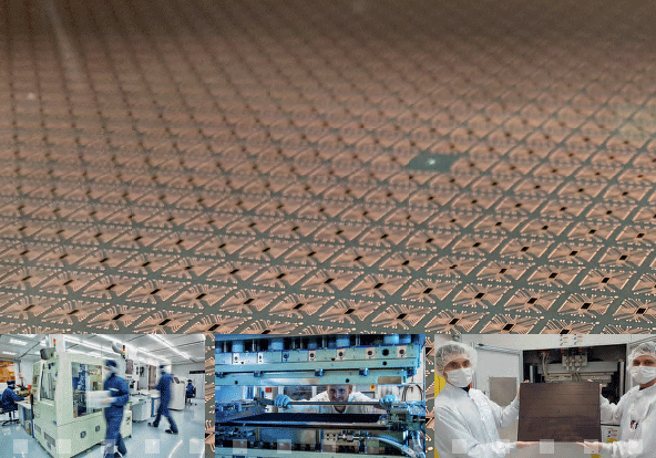
A new technology is now set to do away with this limitation. Fan-out panel level packaging will be the next milestone in packaging technology and a new standard in heterogeneous 3D integration. Instead of round wafers, rectangular panels sized 610 X 457 mm² will be used, allowing the mounting of many more components simultaneously on one substrate. The switch from wafer- to panel-level technology therefore also promises a much higher production volume. The new technology will particularly shape consumer electronics, with its tablets and smartphones, and the market value for this type of packaging is estimated at 170 million USD (Yole 2016).
At home in both worlds
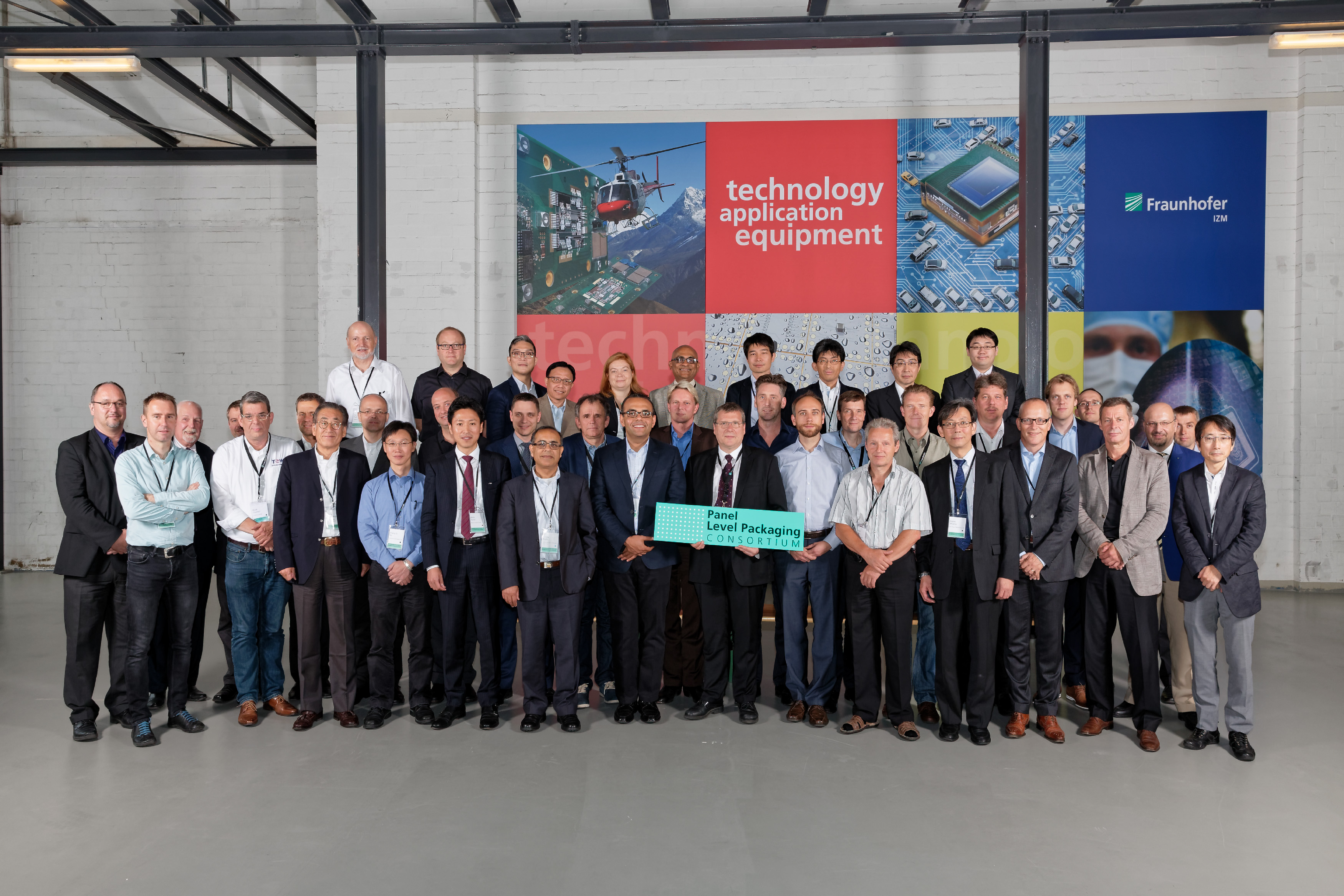
Over the last three years, more than 40 million euros have already been invested into the development of wafer- and panel-level systems at Fraunhofer IZM. “We’re equally at home in both worlds. This makes us unique in terms of the equipment we offer and the techniques we can develop,” explains Dr. Tanja Braun, who is spearheading the technology reemphasis together with Michael Töpper. “We now want to work with leading industry players to develop this process further,” explains the scientist. “A networked processing chain such as here can only be advanced collaboratively.” For this reason, Fraunhofer IZM is currently bringing together a new research initiative, which already includes renowned US, Chinese, Japanese and European companies. The industry and research partners met for the first time on June 28 and 29 for an opening symposium at Fraunhofer IZM in Berlin to discuss the next steps in the collaboration.
Last modified:
 Fraunhofer Institute for Reliability and Microintegration IZM

