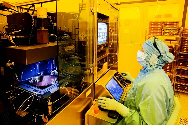
Wafer Level Packaging Line
800 m² clean room (classes 10 to 1000) + 800 m² gray room, 4’’, 6’’ and 8’’, prototyping equipment for some applications also on 300 mm
- Thin-film deposition
- Photolithography (including photo varnishes, polymers and spray coating)
- Galvanic bumping, circuit tracks and through-via filling (Cu, Ni, Au, AuSn, SnAg, PbSn)
- Wet-chemical processes (etching, cleaning)
- Wafer bonding (support wafer, thin-wafer handling)
- Silicon plasma etching (through vias, cavities)
 Fraunhofer Institute for Reliability and Microintegration IZM