PhotonicLEAP
Over five million Euros for photonic packaging and test technologies
PhotonicLEAP, a European Horizon 2020 collaborative research project, has been awarded over €5 million Euros in funding from the European Commission to develop disruptive technologies that will drive down the cost of integrated photonic packaging and test processes.
Photonic Integrated Circuit (PIC) technologies are the light-based equivalent of electronic circuits – a technology that is becoming increasingly important for existing markets in communications, medical devices, sensors and for emerging markets such as quantum computing and security. However, existing PIC manufacturing processes, in particular packaging and test processes, are difficult to automate, with limited manufacturing capacity, and are costly, with packaging and testing typically accounting for over 75% of the total manufacturing cost. As a result, existing PIC manufacturing processes greatly impede the uptake of PIC technologies across many mass markets.
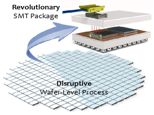
To address this challenge, PhotonicLEAP will develop disruptive wafer-level PIC module integration, packaging and test technologies which will reduce the costs of PIC production by over 10 times, revolutionising existing applications and creating completely new markets.
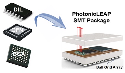
PhotonicLEAP will use these disruptive technologies to produce a revolutionary Surface Mount Technology (SMT) PIC package, which for the first time incorporates multiple optical and electrical connections. The project will validate these technologies through state-of-the-art demonstrators, including a high-speed optical communication module and a medical device for cardio-vascular diagnostics. Furthermore, the technologies will be implemented by the flagship European PIC Packaging Pilot Line, PIXAPP, for future commercialisation. PIXAPP has an extensive and growing user-base across multiple markets.
Fraunhofer IZM is contributing by developing and fabricating functionalized thin glass interposer wafers with up to 200 mm diameter, that will serve as a novel package base for embedding optical PICs and driver ICs, realizing wafer scalable optical, electrical and thermal coupling. Laser structured thin glass will consequentially be used also in closing individual photonic packages - to be used like SMT components as established in electronics.
Prof. Peter O’Brien, Head of Photonics Packaging and Systems Integration at Tyndall and PhotonicLEAP Coordinator, said ‘We are delighted to receive this very significant funding from the European Commission which will enable us to develop truly disruptive photonic packaging and test technologies. The consortium brings a wealth of interdisciplinary skills and state-of-the-art infrastructure to deliver on our ambitious objectives. We are confident the photonic packaging and test technologies developed in PhotonicLEAP can make a real impact to increase the uptake of Integrated Photonics across Europe.”
PhotonicLEAP will be delivered by a highly experienced consortium which consists of six leading research organisations and companies, including Tyndall National Institute, Fraunhofer (IZM & HHI), LPKF Laser & Electronic, ficonTEC Ireland, SUSS MicroOptics, Bosch, Eindhoven University of Technology – TU/e and Interuniversity Micro-Electronics Centrum – IMEC.
(Text: Tyndall / PhotonicLEAP)
Last modified:
 Fraunhofer Institute for Reliability and Microintegration IZM

