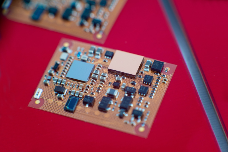
The so-called thin film flex technology offers the same routing density as on chip wafer level redistribution and, at the same time, much greater potential and flexibility for high-density routing than standard thin coreless organic interposers. These polymeric interposers are fabricated with multiple copper routing layers and related inter-layer polyimide dielectric on temporary carrier wafers by repeat metal and polymer deposition and structuring. Depending on the required thickness of the metallization layers, typically in the range of 2 to 5 μm, fine line pitches of currently down to 8 μm can be enabled. The thickness of a single inter-dielectric layer is typically in the range of 5 to 10 μm. As pad finishes, metallizations like Cu, Au, NiAu or solders are available to enable different assembly processes.
As an additional feature, the technology allows the embedding of thin ICs or sensor components into the interposer RDL. To enable that, thin devices with maximum thickness of 20 μm are die-bonded at dedicated positions on the surface of an inner polymer layer. A following overcoating with polymer covers the thin devices completely. To access their I/Os, vias are opened through the top polymer layer and electrical connections are then established by the following wiring layer.
The resulting multilayer build-up is finally detached from the rigid carrier wafer using a high-speed de-bonding process. As a special feature, the technology allows the partial release of the carrier substrate in dedicated areas to create rigid and flexible zones in a single circuit.
 Fraunhofer Institute for Reliability and Microintegration IZM
