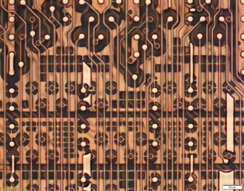
Redistribution (RDL) is a core competence of department WLSI at Fraunhofer IZM and refers to the process of creating an interconnect structure on the top surface of a semiconductor device that redistributes its peripheral electrical I/Os to an area array arrangement. The RDL typically consists of one or more metal tracks (copper, gold or aluminum) and organic (thin film polymers) or inorganic dielectric layers to connect the bond pads on the active device to the new created flip-chip interconnects.
This technology allows a high degree of miniaturization and integration, as it eliminates the need for wire bonding. Wafer level RDL is commonly used in mobile and consumer electronics, automotive, and medical applications, and its popularity is growing due to its benefits in terms of cost, performance, and reliability. Today, single or multilayer redistribution is achieved in a semi-additive process for copper routing down to 2 μm on different substrates, including (ultra-thin) silicon, glass (glass interposer with TGV’s), III – V semiconductor, SiC, or epoxy mold compounds (EMC).
Design variants can be realized on wafer level by using a mask aligner with full-field exposure masks or laser direct exposure (355 nm). The RDL technology is used to produce CSPs with fan-in and fan-out routing, substrates with high density routing as well as TSV or polymeric interposers.
 Fraunhofer Institute for Reliability and Microintegration IZM