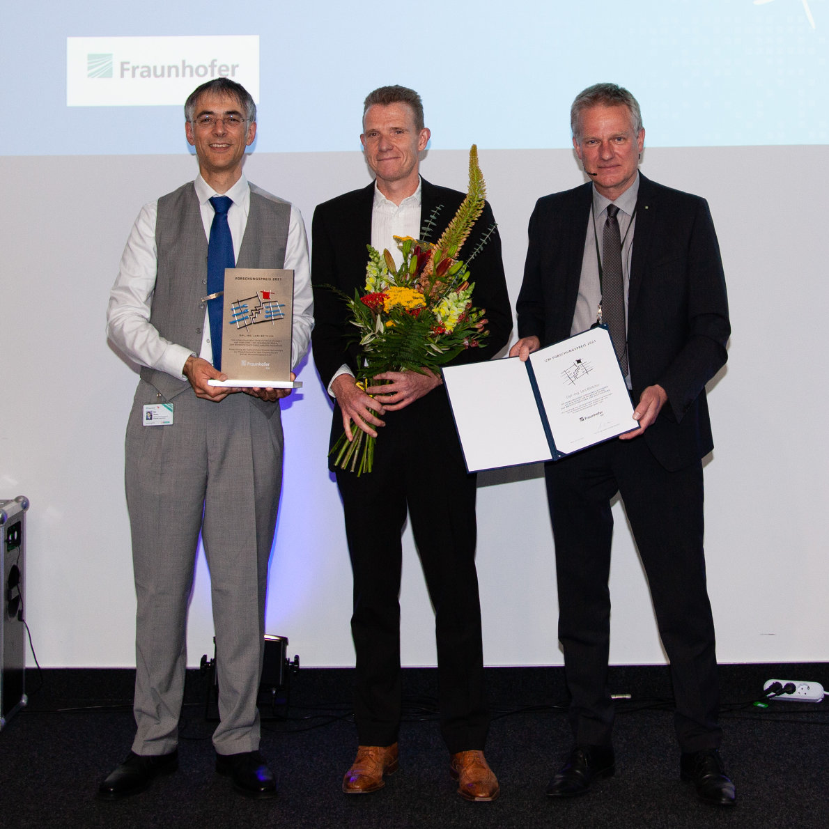
Lars Böttcher presented with Research Award for chip embedding technologies
For over two decades, Lars Böttcher has helped electronic systems become smaller, more reliable, and better at handling high frequencies through his work on embedding chips in circuit boards. With his team and many industry partners, he has brought the former niche technology into the mainstream and paved its way into exciting new applications in the automotive sector, medical technology, or even consumer electronics. In recognition of these efforts, he was chosen as the recipient of the 2021 Fraunhofer IZM Research Award. Due to the COVID pandemic, the official presentation was postponed until June 23, 2022.

Chip embedding has been a game changer for the development of miniaturized electronics. Its success relies on a smart change in where microchips are located on circuit boards: Conventional approaches would have the chips mounted on top of the board, but embedding sees them laminated right into the circuit board itself. This produces highly compact components with numerous advantages over the standard technique.
Compared to conventional designs, embedded chips are far more durable, as the fragile and sensitive semiconductors are fully enclosed by the circuit board’s fabric. They can be located in close proximity to other components for shorter lines of communication, or even stacked on top of each other to produce miniature 3D systems.
The technology also gives developers a much freer rein to try other materials. Conventional chip contact approaches like wire binding can use several metals for wires and solders, like aluminium, copper, or silver, but the combination of materials and the complex geometry of conductors and bond wires can cause certain parasitic effects that are detrimental for the system, especially at high frequencies. Embedded chips, by contrast, simply use direct copper contacts – an excellent option for applications with high switching frequencies.
The new millennium had only just begun when the microsystems specialist Lars Böttcher recognized the immense potential of embedding technologies and began to research concepts for packaging chips in polymers at Berlin’s Fraunhofer Institute for Reliability and Microintegration IZM. Moving chips from the surface into the actual fabric of the circuit boards opened up untold opportunities for Europe’s industry. The technique not only allows developers to reduce the size of their designs substantially. It also gives them great creative freedom, combined with improved reliability, better electrical performance and, not least, much more economical production processes. These and other advantages helped establish the technology as a go-to option in the industry, especially for power electronics.
Working at the forefront of these developments, Lars Böttcher and the 28 people in his “Embedding & Substrate Technologies” research group are combining standard circuit board technology with surface-mount (SMT) approaches and chip embedding to produce contact pitches of a mere 50 micrometres with exceptional reliability and excellent properties. Components can ultimately be embedded in two basic alignments: “face-up” or “facedown”, indicating the direction of the chip contacts. Both are common and viable options for circuit board designs, but each has its unique properties and advantages. For vertical components, such as diodes or power MOSFETs, Böttcher’s team at Fraunhofer IZM prefers orienting the chips face-up.
Even after decades in the field, the embedding specialist is not worried about reaching the end of the line with his research. The field keeps evolving as novel applications come into focus all the time. High-frequency technologies demand new, reliable solutions. High-density wiring is needed for panel-level packaging. Modern power electronics have to accommodate modules that can handle several hundred kilowatts going through them. And long before real-world applications even begin to matter, developers are exploring novel materials, like organic substrates, and need to know how they fare when it comes to embedding. The Fraunhofer Research Award has been given out for “exceptional research in the field of microelectronics, microsystems engineering, and packaging” for more than twenty years. It honours research excellence and, above all, the successful application of new research in industrial use. Due to the COVID pandemic, the formal presentation of the award to Lars Böttcher did not take place until June 23, 2022.
About Lars Böttcher:
For more than two decades, Lars Böttcher has been researching and developing new technologies with a special focus on metallization, photolithography, and laser technology at the Fraunhofer Institute for Reliability and Microintegration IZM in Berlin. As head of the Institute’s “Embedding & Substrate Technologies” group, he is in charge of both publicly funded and industrial projects. He is an active member of the International Microelectronics And Packaging Society (IMAPS) and the Surface Mount Technology Association (SMTA), where he is working to promote progress in packagingand substrate technologies.
(Text: Olga Putsykina)
Last modified:
 Fraunhofer Institute for Reliability and Microintegration IZM