Fraunhofer Institute for Reliability and Microintegration IZM
Fraunhofer President experiences semiconductor research in Dresden
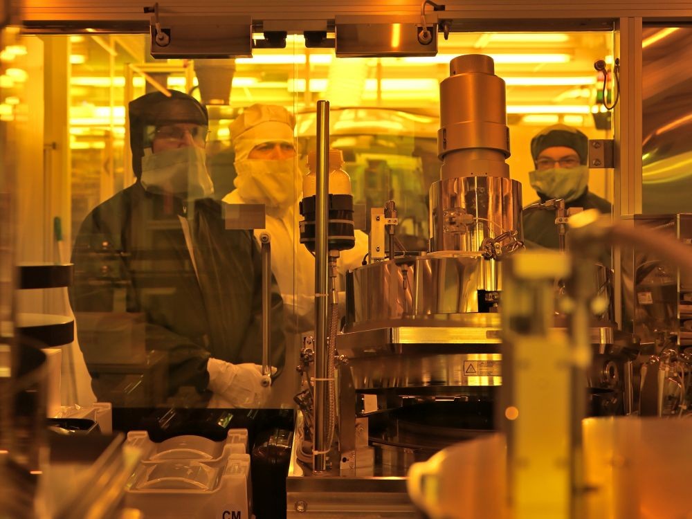
Continuing last year’s whistle stop tour of Fraunhofer sites in southern Germany, the society’s new president, Professor Holger Hanselka, has come to Saxony to visit the institutes in and around the state capital of Dresden. Fraunhofer IZM-ASSID invited him into its cleanroom to experience the strong partnership between industry and research that the site has been known for in the last 15 years.
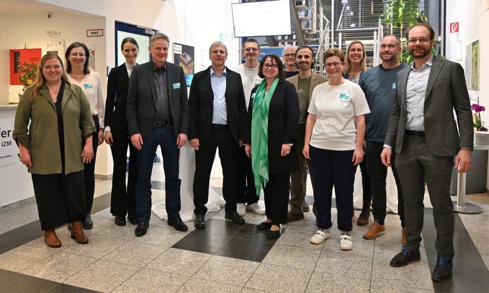

„It is this culture of genuine cooperation at Fraunhofer that I want to build on. Listening to each other is essential for any constructive change“, Professor Holger Hanselka, chosen in August as the 11th Fraunhofer President, said at the start of his inaugural trip which is taking him to a selection of the many Fraunhofer sites.
Following his visit to Fraunhofer IPMS near Dresden airport, the stop at Fraunhofer IZM-ASSID gave the society’s new president a chance to see the „pilot production of detectors for the latest generation of computer tomography scanners based on wafer technologies" in the cleanroom. Site manager Dr. Manuela Junghähnel and Fraunhofer IZM’s overall director in Berlin, Professor Martin Schneider-Ramelow, explained the mission of the site and the expansion plans for the Center for Advanced CMOS & Hetero Integration Saxony (CEASAX) in cooperation with Fraunhofer IPMS-CNT. Hanselka was enthusiastic about what he saw: „These facilities not only show us that we, as Fraunhofer, have to play a key role for the EU Chips Act, but that we have actually been doing so for a long time.“
Microelectronics research in particular is becoming increasingly important in Dresden. The major chip foundries are establishing themselves in the region, and cooperation with other enterprises in the semiconductor industry has been intensifying for several decades already. Two Fraunhofer institutes seized this moment as an opportunity to combine semiconductor research on 200/300 mm silicon wafers in shared cleanroom facilities. More info
Last modified: