 Fraunhofer Institute for Reliability and Microintegration IZM
Forging the last link in the process chain – Fraunhofer IZM manages to automate measuring optical in-glass waveguides
The use of glass as substrate in electronics manufacturing enables the additional transmission of optical signals through the substrate material. This allows much higher rates of data transmission, which is vital for many scenarios like automotive, telecommunication, or AI applications. Researchers at Fraunhofer IZM have now managed to develop a system that can automatically measure propagation losses in integrated optical waveguides, all part of the research project “Integrated Electro-Photonic Panel Systems” (EPho).
The rapid growth of data volume in our increasingly digitized world calls for new solutions for the efficient processing and transfer of data. This means chips with even more transistors, tiny electrical components that are responsible for calculations. This is especially relevant for high-performance computers and datacenters, where the largest amounts of data have to be processed. But the miniaturization of transistors and their electrical connections is hitting the limits of what is technically possible. The smallest structures on modern chips already consist of only a few atoms of silicon. This type of precision requires rigorous conformity and exactitude during manufacturing, leading to smaller production yields at significantly higher cost.
To economically increase the number of transistors on a chip and keep Moore’s Law alive, increasing efforts have concentrated on distributing transistors across so-called “chiplets” instead of placing them all on one chip. This paradigm change has long been expected in the industry*¹. However, chiplets can only become a feasible option with effective chiplet interconnections.
The choice of substrate is becoming increasingly critical: The connections between the chiplets must fit into ever tinier spaces. With the current target of 3μm (line/space), organic substrates are reaching the limit of what can be reliably processed. The industry’s leaders like Intel are now looking to glass as an alternative substrate. Fraunhofer IZM has long been exploring electrical connections on glass, as glass also allows optical waveguides to be integrated. This means that electro-optical circuit boards can transmit not only electrical, but also optical signals and, as a result, massively boost data transmission rates.
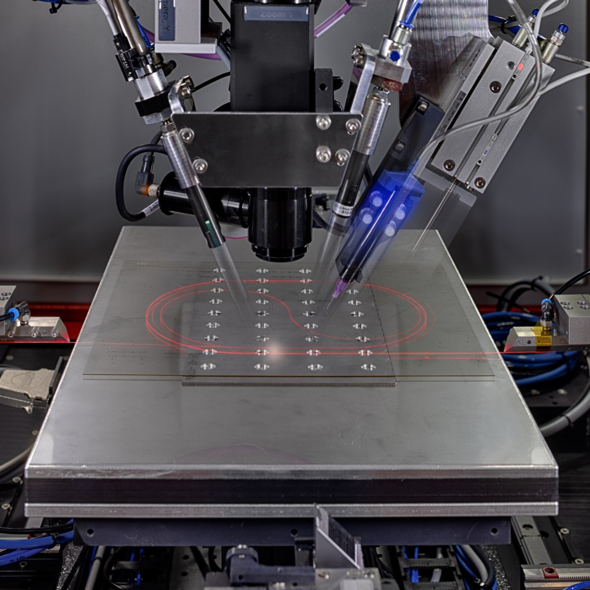
Fraunhofer IZM has developed an ion-exchange process using commercial equipment to produce low attenuation single and multi-mode waveguides on large format (>450mm x 300mm) thin glass (<550μm) panels. As a single panel can have many hundreds of waveguides, inspecting and characterizing such panels is a challenging and time-consuming task, not least because, unlike electrical circuits, optical waveguides can cross each other and form extremely complex layouts on a single panel. To facilitate the complex process chains needed to produce such panels, a platform was developed to automatically determine the propagation loss of integrated waveguides. It can accommodate even waveguides created by femtosecond lasers or waveguides in other substrate materials. The procedure remains the same in every case:
1. A sample is loaded into the system.
2. The layout is uploaded, the user selects the waveguides to be measured, and the measurement starts.
3. The platform automatically detects the edges of the substrate, any existing marks, as well as the exact position of the measurement fiber before taking a reference measurement. It then uses this information to calculate the insertion losses of all automatically measured waveguides.
The system developed here gives manufacturers complete control over the production process of optical waveguides. In addition, many thousands of parameter sets can be analyzed to help define new parameters for improved optical waveguide production processes. The system can speed up progress developments substantially, especially for technologies that need to contend with many variable parameters, as is the case when laser-cutting waveguides.
The EPho project (16ES0806) was brought to a successful conclusion in 2022, supported by EUR 1.33 million in funding from the Federal Ministry of Education and Research (BMBF) to the amount of 1.33 million euros. Additional partners on the project included ILFA GmbH, Schröder Spezialglas GmbH, and FiconTEC Service GmbH.
*¹ Read the RealIZM interview with Dr Michael Töpper of 5 September 2019: https://blog.izm.fraunhofer.de/..

Last modified: