Thin film polymers are used as compliant layers and interdielectric layers for Wafer Level Packaging (WLP), Panel Level Packaging or Sensor Packaging. The processing and the properties of the polymers show a distinct impact on the reliability of Fan-In and Fan-Out packages.
Fraunhofer IZM offers polymer processing services as well as thin film polymer characterization. We can reference on a processing experience with thin film polymers of over 25 years. Our clean room is equipped with production-like tools on which we can process various types of thin film polymers like:
- Polyimide (PI)
- Benzocyclobuten (BCB)
- Polybenzoxazole (PBO)
- Epoxy
- Acrylate
- Resist
For processing of liquid type polymers, Fraunhofer IZM has automated or manual spin coaters for wafer sizes between 3 inch and 300 mm as well as spray coaters for substrates with topography up to a substrate size of 610 x 475 mm2 (24x18 inch2).
For 3D packaging and fluidic applications, dry films become increasingly popular. Fraunhofer IZM can laminate dry film in hot roll process for 150 mm and 200 mm wafers (carrier to carrier automate). Also, a vacuum lamination for small pieces or up to samples sizes of 610 x 475 mm2 is possible.
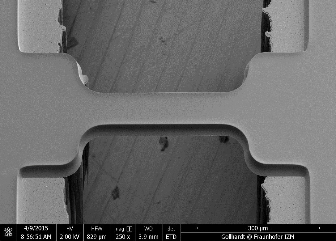
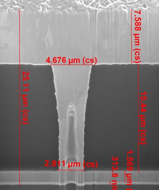
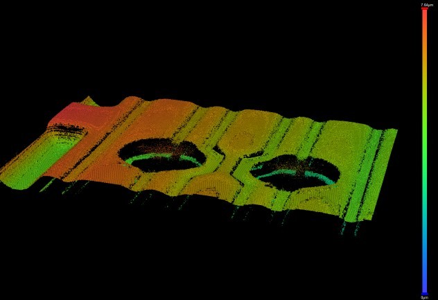
Exposure of thin film polymers can be done by mask aligner as well as by a maskless laser direct imager with a possible resolution down to 0.75 µm. Non-photosensitive materials can be structured by direct excimer laser ablation (248 nm) as well as plasma etching (reactive ion etching, RIE) up to 300 mm wafer size.
The polymerization reaction can be done in nitrogen ovens with a maximum temperature range of over 450°C at Fraunhofer IZM.
Polymers can be evaluated for customer-specific applications and we have close cooperations with material suppliers to find the best fit. The polymeric layers can be evaluated and characterized with respect to their properties e.g.
- Measuring the Young’s modulus,
- Tensile strength
- Elongation to break
- Coefficient of thermal expansion
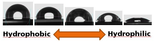
- Water uptake and permeability
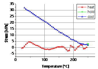
- Mechanical stress (-50°C to 500°C)
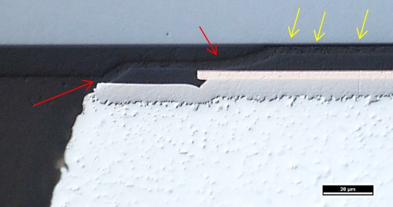
- Adhesion to different materials
- Degree of polymerization using FT-IR spectroscopy
- Curing profile using DSC
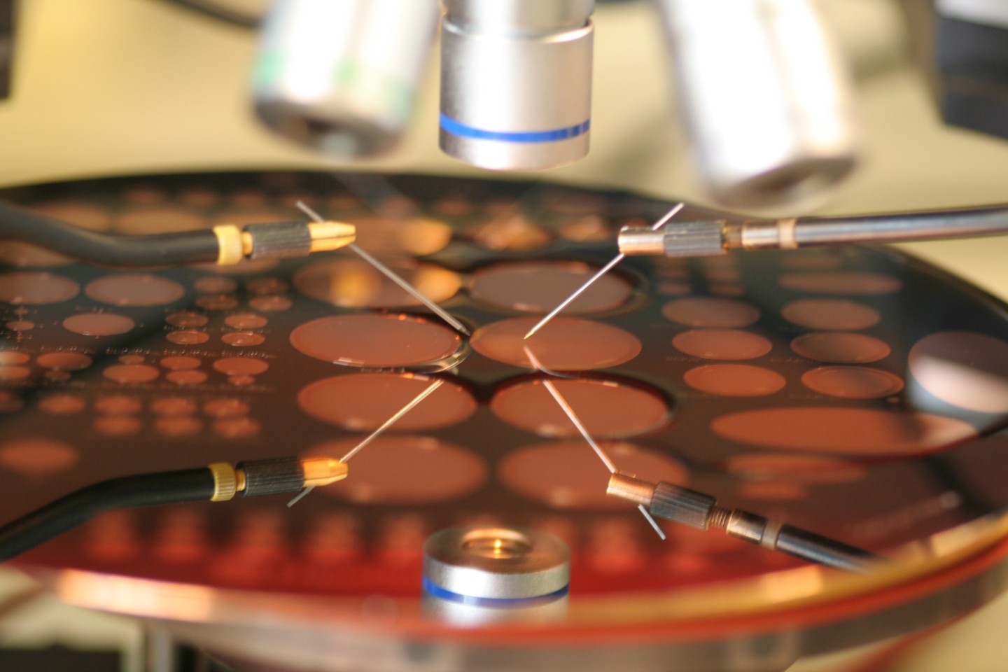
- Copper ion migration (HAST and bHAST with interdigital capacitors with 2/2 µm Lines and Space)
- Electrical properties at frequencies up to 110 GHz like dielectric constant, loss factor
- Break down voltage (TDDB time dependent break down voltage).
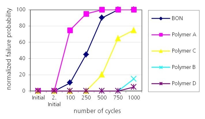
- Second board level reliability like air to air thermal cycling (AATC) and drop test
- Process evaluation on various substrates like Silicon, glass, ceramic and epoxy mold compound (EMC)
Based on our long term experience, Fraunhofer IZM provides market researches and overviews as consultant service. In workshops we offer trainings for lithography processes and polymer material applications for advanced packaging.
A literature data base is available at Fraunhofer IZM for widely used low-k polymer BCB.