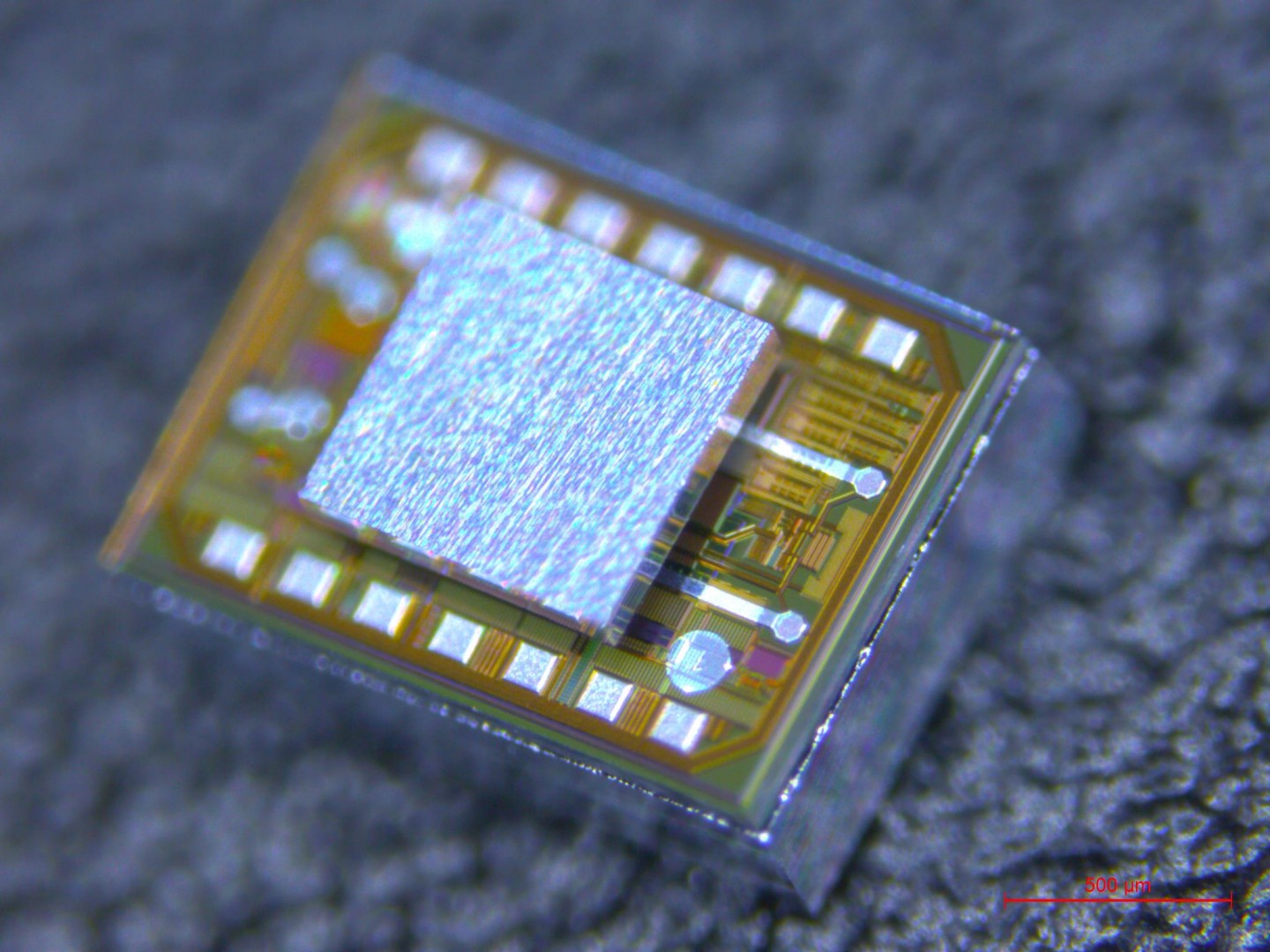
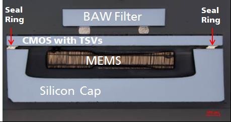
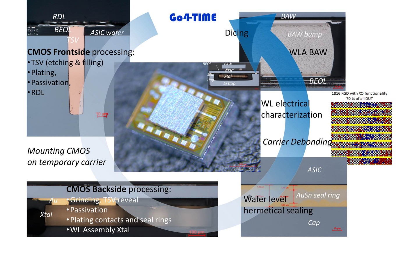
Together with its industrial and academic partners, Fraunhofer IZM develops base technologies for the wafer level fabrication of low-cost, miniature, chip-scale packaged (SCP) hybrid microsystems.For this purpose, standard technologies like redistribution, TSV formation and wafer to wafer bonding are combined to obtain versatile approaches for hermetic wafer level packaging of MEMS components. Within the project Fraunhofer IZM evaluated the described approach for wafer level packaging of generic timing micro systems. The systems include a special designed timing ASIC build in TSMC 180 nm technology, a miniature quartz tuning fork with 131 kHz resonance frequency as well as a 2 GHz bulk acoustic wave (BAW) filter device.
The ASIC wafers were processed with 100 µm deep Cu TSVs in a front side via last regime. During back side processing of the ASIC wafers proper gold structures for assembly of the quartz components and gold/tin frame structures for bonding of the cap wafers were ceated.
The fabricated cap wafers had a thickness of 400 µm. On these wafers, gold metal frames which match in pitch and lateral dimensions to the frames at the AISC were created. Inside these frames 200 µm deep recesses were etched to generate space for the quartz crystals. Both, ASIC and cap wafers were bonded together in vacuum with standard wafer bonding equipment using a gold/tin soldering regime. After the wafer bonding step, the BAW filter devices were mounted on the ASIC wafer front side using reflow soldering.
Depending on wafer format, with such a wafer level packaging approach up to several 10k MEMS devices can be hermetically packaged in parallel at one wafer.