 Fraunhofer Institute for Reliability and Microintegration IZM
We help companies develop energy-efficient sensor, communication, and radar systems more quickly, identify technological risks early on, and safely bring innovations to market.
High-Frequency Microelectronics Laboratory: Development, Testing, and Validation of High-Frequency and Sensor Systems
Equipment
Electronics today have to be more powerful, energy-efficient, and reliable than ever before. At the same time, more and more is expected in terms of development time, product quality, and resource efficiency.
The High-Frequency Microelectronics Laboratory supports companies in overcoming these challenges. We analyze materials, characterize high-frequency components, validate new technologies, and optimize the energy consumption of electronic systems as early as the very first development phases.
From the initial idea through prototyping to proven technology, our partners benefit from state-of-the-art laboratory infrastructure, scientific excellence, and many years of experience gained from research and industrial projects.
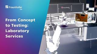
Privacy warning
With the click on the play button an external video from www.youtube.com is loaded and started. Your data is possible transferred and stored to third party. Do not start the video if you disagree. Find more about the youtube privacy statement under the following link: https://policies.google.com/privacyWhat challenges can we master?
- When developing new sensor and high-frequency systems, companies often face key questions:
- How can a system’s energy consumption be minimized already in development?
- Which materials, designs, and manufacturing processes offer the best performance?
- How reliably do sensors and radar modules function under real-world operating conditions?
- Where are the vulnerabilities that could lead to future failures or performance losses?
- How can development be accelerated and costly design flaws be avoided?
- We provide reliable answers through precise measurements, data-driven analyses, and practical validations.
Our R&D Services
- Development of energy-efficient radar front-end modules and sensor systems
- Circuit analysis and design review
- System testing, commissioning, and technical failure analysis
- Validation of ultra-low-power software and firmware
- Analysis and optimization of power consumption down to the microampere range
- High-frequency characterization of components and systems
- Support for the integration of new technologies into applications
Our Expertise
- Material characterization of waveguides and high-frequency modules up to 1 THz
- Antenna characterization up to 330 GHz
- S-parameter measurements up to 330 GHz
- Evaluation of high-frequency components for demanding application scenarios
- Analysis of energy efficiency and system performance at the component and system levels
- Commissioning and testing of embedded systems and wireless sensor systems
State-of-the-art infrastructure for precise results
Our laboratory and measurement technology enables the precise characterization and evaluation of materials, components, and complete systems across a wide frequency range.
Equipment (excerpt)
Antenna characterization
- Low-reflection antenna test chamber with a spherical robotic scanner for the complete 360° characterization of antennas: NSI MI7000
- Near-field measurements from 18 GHz to 40 GHz and far-field measurements from 40 GHz to 320 GHz
- Supported antenna interfaces: RF connectors, waveguides, or GSG (Ground-Signal-Ground) probes
Material characterization I Frequency range from 1 MHz to 1 THz
- Fabry-Pérot resonator with a frequency range from 18 GHz to 140 GHz
- Free-space setup up to 70 GHz
- Vector network analyzer with frequency extensions up to 500 GHz
- Impedance analyzer
- Various resonators
- Quasi-optical test bench
- THz spectrometer
On-wafer measurements
- Semi-automatic 300-mm probe system for on-wafer measurements up to 330 GHz (temperature range: −60 °C to +200 °C)
- Two manual 200-mm wafer probers for measurements up to 330 GHz and temperatures up to 300 °C
High-speed signal analysis
- Arbitrary waveform generator with 64 GS/s
- Spectrum analyzer up to 50 GHz
- Modulators/demodulators up to 330 GHz
- Bit error rate tester up to 64 Gb/s
- Sampling oscilloscope up to 80 GS/s
Energy and power characterization
- Precision multimeters for high-accuracy voltage, current, resistance, capacitance, and temperature measurements (10 nV, 1 pA, 1 μΩ, 100 fF, 3 Hz, 1 m°C)
- 4-quadrant power supply for arbitrary supply and load profiles
- Automated test bench for the long-term measurement of energy balances and functional reliability
- LCR meter for component characterization
- Logic analyzer for common digital interfaces (e.g., I²C, SPI, UART, and RS485)
Your Benefits
Why partner with us
- Recognize and reduce development risks early on
- Optimize RF, ultra-low-power, and embedded systems through targeted fault analysis and validation
- Optimize energy consumption at an early stage in the development process
- Accelerate development with strong measurement data and validations
- Translate new technologies faster into market-ready applications
Bringing innovations to market faster through collaboration
Whether it is energy-efficient sensor technology, high-performance radio frequency modules, or cutting-edge radar technologies: We help you master technical challenges, minimize development risks, and realize the full potential of your innovations.
Come and speak to us about your project. Together, we will develop solutions that turn scientific insights into commercial success.
Frequently Asked Questions (FAQ)
What high-frequency measurement services does the lab offer?
We perform material, antenna, and S-parameter measurements up to the THz range.
Which applications is antenna characterization suited for?
Radar, communications, sensor, and IoT applications.
Does the lab also support companies with prototype development?
We support projects from the initial design concept through to the development of their first prototypes and small-batch production to the qualification of the technology.
How does the lab help with energy optimization?
We help by analyzing energy consumption, validating ultra-low-power systems, and identifying opportunities for optimization.
How does the lab support the development of energy-efficient embedded systems and wireless sensor systems?
Using state-of-the-art measurement technology, we enable a systematic and comprehensive analysis of the energy requirements of components, assemblies, and complete systems. The data we obtain forms the basis for optimal system partitioning and can contribute significantly to the energy efficiency of IIoT systems. This can help pinpoint functions that could be implemented more energy-efficiently in hardware than in software. Our final validations verify the impact in terms of energy consumption and functional reliability.