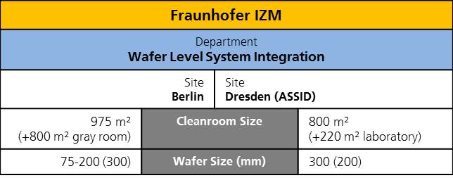
The department "Wafer Level System Integration" (WLSI) develops advanced packaging and system integration technologies and offers customer-specific solutions for microelectronic products in the overall scope of smart system integration. Approx. 60 scientists work at two locations: Berlin and Dresden (ASSID: All Silicon System Integration Dresden). WLSI is cooperating globally with manufacturers and users of microelectronic products as well as cleanroom equipment producers and material developers from the chemical industry.
Wafer Level System Integration
Tabbed contents
Key Reseach Areas
Research areas of the department WLSI:
Services
2.5/3D Technologies
- TSV Integration
- Silicon interposer TSV first
- TSV via middle
- TSV via last
- Device stack
- Glass interposer and TGV Integration
- 2.5/3D Interposer
- Backside Interconnects
- 3D Stack Formation
- Flexible High Density Multi-Layer Substrates
- Polymeric interposers based on thin film flex technology
High Density Redistribution
- High Density Redistribution
- Multi-layer Redistribution
- Polymers for high-density Interconnects
- Copper/Polymer Evaluation Kit
- Integration of passive devices
- Glass substrate and layers
- Fan-out Wafer-Level Packaging
- High-Density-Routing (RDL)
Wafer-Bumping
- Wafer Bumping via Electroplating
- Solder & pillar bumps
- Fine-pitch bumping for Pixel Detectors
- Fabrication of nanoporous old Structures
- Mechanical gold stud bumping
- Single chip bumping
- Electro chemische deposition
Wafer-Bonden
- Permanent wafer-to-wafer bonding
- Temporary wafer bonding for thin wafer handling
- Wafer level capping
Thinning/Singulation/Dicing
- Back grinding tape lamination
- Wafer backgrinding
- Polishing
- mechanical blade dicing
- laser grooving
- laser stealth dicing
- wafer edge trimming
High-Density Assembly
- Fine pitch assembly for pixel detectoren
- Detector packaging for medical x-ray imaging and x-ray crystallography
- Interconnect metallurgy and processes
- Thermo compression bonding
- Chip-Stacking
- Fine-pitch flip chip (FC) assembly & die bonding
- Wafer-level solder ball attach (100 – 500 μm)
- Evaluation of low-temperature assembly technologies
- Evaluation of flux free solder connections with self alignment capability
- Reliability investigation of flip chip interconnections
- Chip to Wafer Assembly
Failure Analysis & Reliability Investigation
- Metrology: Bump heights / TSV depth measurement, defect inspection, topology, layer thickness, wafer thickness & bow/ warp (VIS), wafer thickness (infrared), die warpage measurement, physical failure analysis, preparation techniques 3D stack
- FIB / REM imaging
- Copper/polymer evaluation kit - Interdigital finger-type capacitors
Sensor Development
- Sensor design
- Reliability and lifetime optimization
- Standard and customer-specific packaging with integrated sensor data processing e.g. TO8, packages with media separation, molding
- Characterization of pressure (10 m-100 Bar), gas and acceleration sensors (up to 40 g)
- Planar technologies (SiO, SIN deposition, Sputtering)
- Overview sensor activities
Photonic & Plasmonic Systems
Equipment
The department WLSI has cleanrooms and laboratories with production-compatible equipment available at both sites. Beside the flexibility regarding the processing of different wafers sizes, both process lines are also characterized by a high adaptability of the individual processes. The process line at ASSID is particularly tailored to realize production-related and industry-compatible development and processing.
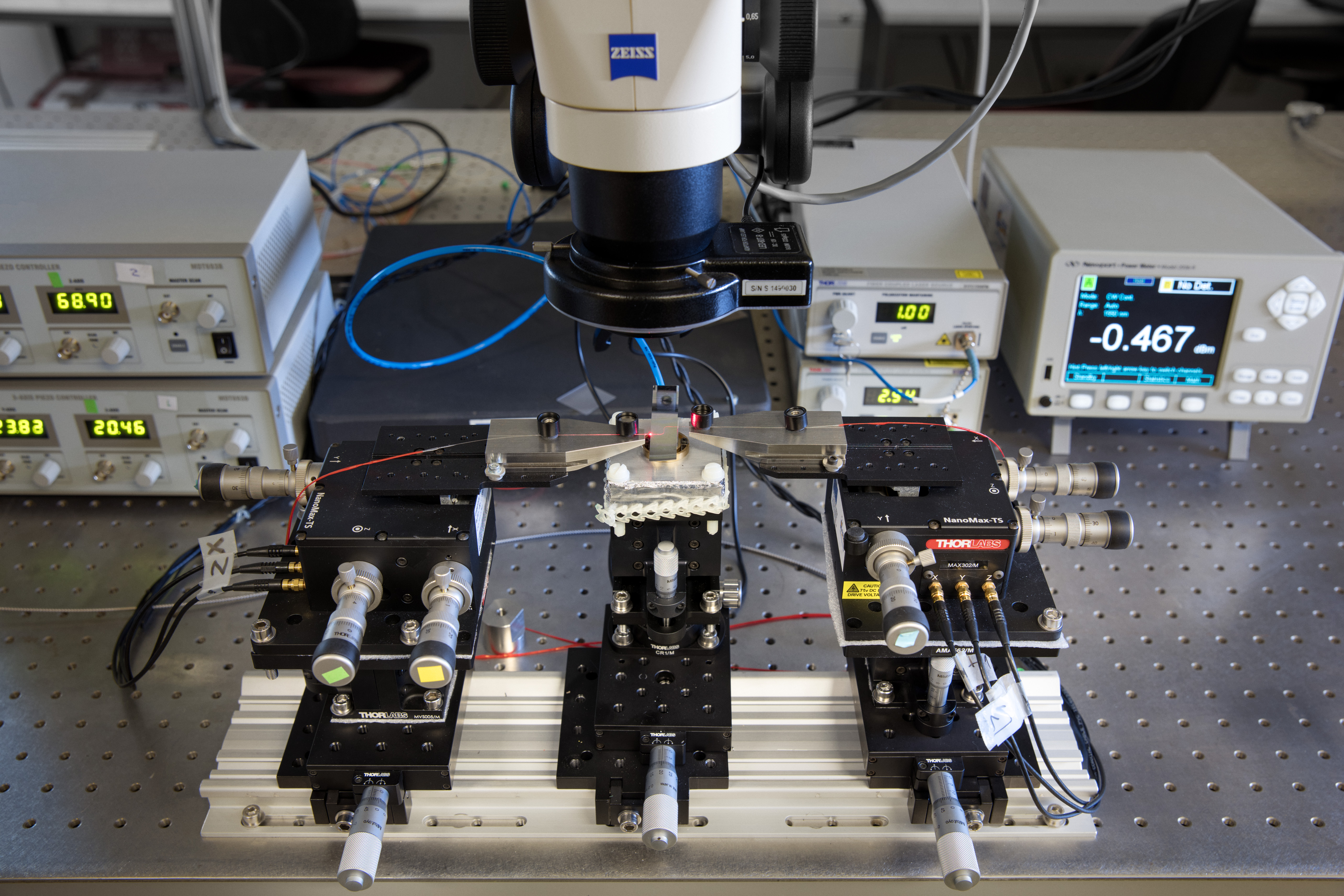
Furthermore, in Berlin we have with our PhoxLab an independent and neutral platform for benchmarking and presentation of photonic components and solutions for various hirachy levels, architectures and protocols in data centers.
Technology & Project Information
Data & Technology Sheets
Project Information
 Fraunhofer Institute for Reliability and Microintegration IZM

