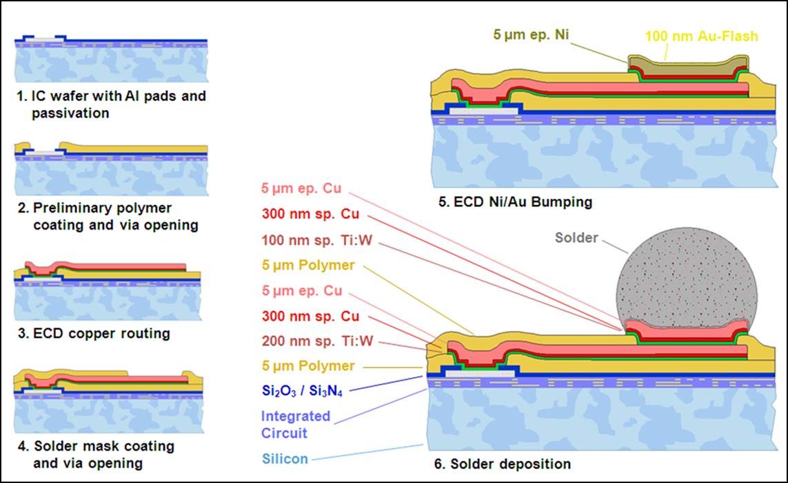
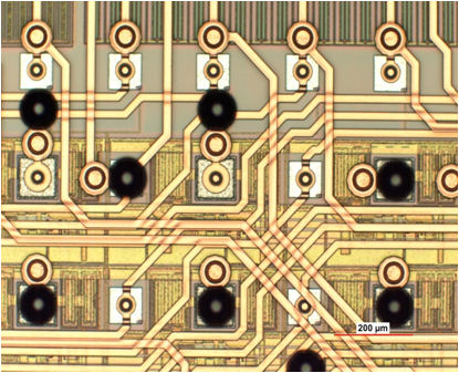
The electrical connection between a semiconductor chip or a sensor to the next level of packaging (i.e. the substrate) can be achieved by wire bonding, glueing or soldering. The final metallization on the components for these interconnection are Al, Cu or Au. A modification is needed if soldering will be used to guarantee a reliable interconnection. Therefore a so called under bump metallurgy (UBM) is deposited which consists of a diffusion barrier and an adhesion layer. The solder (SnAg, SnAgCu, PbSn, AuSn, or others.) is deposited in a further process step. There is one limitation for the flip chip assembly on a board: The fine pitch of the electrical contacts on the die. These contacts are located at the periphery of the chip as a standard for wirebonding technology. Only most of the microprocessors have an area array configuration because they are fc bonded due to the enormous amount of contacts (up to server thousands). This area array configuration enables a relaxed grid for the solder interconnection to the board being limited to the amout of contacts and the chip size.
This process bridging the peripheral contacts to an area array configuration by a thin film metallization is called redistribution technology. Different type of thin film polymers can be used as isolation and passivation layers: BCB, PI, PBO, Epoxy or even Glass. The required metallization is deposited by sputtering an adhesion and diffusions barrier of TiW or Ti and a plating base of Cu. Full field lithography (mask aligner) is used to pattern a thick photo-resist for the subsequent electroplating process of Cu deposition. Line and spaces of down to 3 µm can be achieved. Up to 15 µm thick Cu can be plated depending on the wiring density. In addition inductive elements like coils can be added into the wiring system. The deposition of the solder can be done by an addition plating step or by mechanical bumping methods like ball drop or stencil printing. Therefore the size of the bumps can be varied between 20 µm and hundreds of microns. All established solder compositions like SnAg, SnCu, SnAgCu, PbSn, AuSn but also pure Cu of Au are within the process specifications. The components are ready for assembly after singulation by dicing. The assembly can be done with or without underfiller depending on the chip size and the required reliability requests. Test chips of different sizes and pitches for the evaluation of this technology are obtainable at Fraunhofer IZM.
Technological compentencies
- Multi-layer redistibution
- Polymers for high-density redistribution
- Integration of passive components
- Glass substrate and layers