Integration of Passive Components into Thin Film Multi-Layer
Increasing functionality and decreasing system volume are the major trends for portable electronic products like smart phones, personal digital assistants or multi-media devices. In order to keep this trend ongoing the concept of Hetero System Integration is applied, meaning that different but highly specialized technologies have to be used for the realization of the different partitions of the entire system leading to highest packaging densities.
In this context especially the passive components, which are mainly assembled as discrete components today, are getting more and more into focus. Since they can make up most of the total volume, the total number of interconnects and the assembly costs of the whole system, one promising approach is their realization as integrated components within the ICs, interposers or additional sub-components of the system.
Fraunhofer IZM offers different approches to integrate passive components like inductors, capacitors and resistors into thin film multi layer wiring or redistribution layers on different types of substrates. The components can either be integrated into redistribiution layers on active ICs or silicon interposers as well as on passive substrates like blank silicon, glass or ceramic wafers.
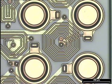
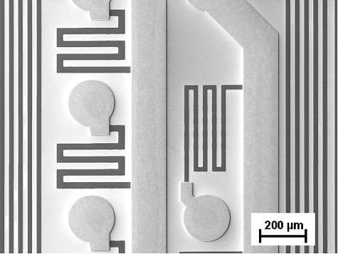
Single and double layer inductors are realized by using at least two metal layers, who are separated by one dielectric insulation layer. Depending on the electrical requirements square, round, octagonal or arbitrary winding shapes can be done with line widths and spaces down to 4 µm and height to width aspect ratios larger than 1. Due to using electroplated copper as conductive and low loss polymers as inter dielectric layers, high quality factors can be obtained.
The same layer construction is used to fabricate small value metal-insulator-metal capacitors suitable for RF and timing applications. Due to the low dielectric constant of the polymer dielectric the capacitance density is low and in the range of some pF/mm2. In order to obtain higher capacitance densities, the regular polymer is replaced by other paradielectrics such as thin glass or tantalum oxide layers. In this case capacitance densities up to several nF/mm2 are possible.
For thin film resistor integration sputtered Nickel/Chromium (NiCr) with a sheet resistance of 100 Ohm/square is used. The NiCr is structured by negative technology using wet etching to create resistor meanders with minimum line width of 10 µm. Thus total resistance values between 100 Ohms and several hundred kOhms can be fabricated.