Design and Simulation of Optical and Electrical Systems
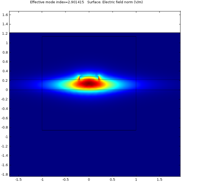
Simulation of Si waveguides
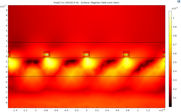
Simulation of plasmonic grating couplers
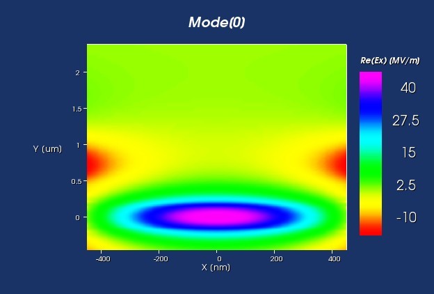
Simulation of TiO2 waveguides
Design and simulation are the foundation of any stable, well-prepared project. Particularly the high frequency demands of photonic systems pose high challenges. Apart from a comprehensive understanding of the nature of photons and all their interactions, a broad understanding of the electrical path is required. Moreover, simulation has to not only work under lab conditions, but also in the real world, under influences like temperature, humidity and electromagnetic disturbances.
We use different tools and combine them as needed, like:
Electromagnetic Simulations
- RF and wireless design
- PCB/EOCB design
- Thermomechanical
- 3D packaging
- Signal integrity
- System in Package (SIP)
Photonics
- Full set of passive and active building block design for different platforms (SoI, Si3N4, Polymer, Glass and InP)
- Plasmonics: CMOS-compatible optical building blocks