Waveguide coupler - Nanosystec

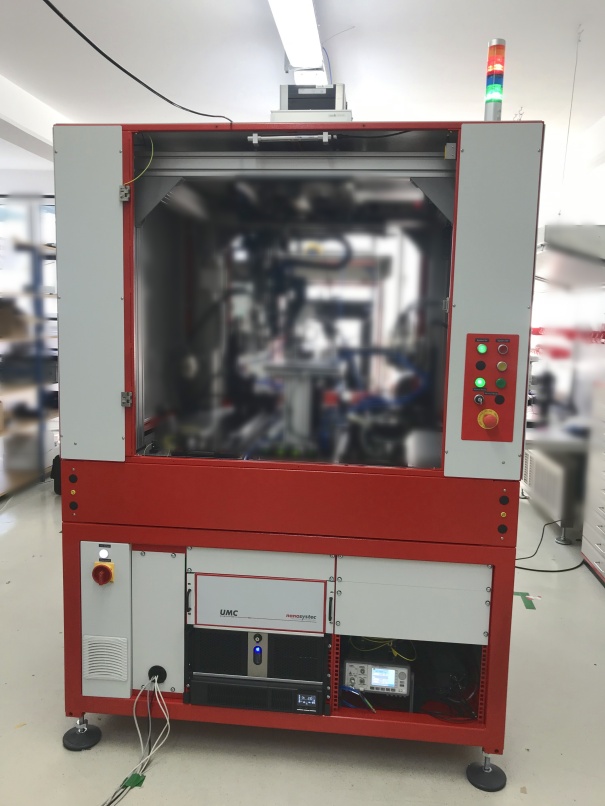
Fig. 1: Automated system for optical measurements of integrated photonics and fiber assembly

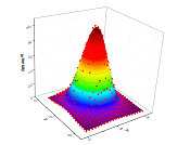
Fig. 2: 2D-MFD Scanning of a fiber
The high demand for miniaturization of optical systems in a wide spectrum of applications, including quantum technology, is driving the development of integrated photonics with an increasing number of waveguides per chip or panel. Automated equipment for measuring and connecting optical fibers to chips and panels is therefore essential. At Fraunhofer IZM we have an EFRE-funded facility with the following features:
- Automated routines for optical characterization (IL and MFD) of a high number of waveguides
- Edge and vertical coupling with an axis resolution of 50 nm
- Software-controlled, precise placement of adhesive drops and their curing with a UV light source
- Detection of marks with an integrated camera and automatic light coupling into the waveguides using special algorithms
- Substrate:
- Panels: size up to 457 mm x 305 mm with SM or MM waveguides for 1310 nm und 1550 nm
- Chips: Design with SM or MM waveguides and different platforms (e.g., Polymer, Si and SiN)
- Single fiber or Fiber array:
- Standard (SM/MM) and polarization maintaining fibers
- Lensed und UHNA-Fiber
 Fraunhofer Institute for Reliability and Microintegration IZM