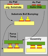
For the flip chip bonding of III/V semiconductor devices (GaAs, InP) such as FET, HEMT, MMIC and optoelectronic components mechanical Au-bumping is available as a single chip process or for bumping of substrates.
Since the Au ball bumping is performed using a modified wire bonder, the process is very flexible and suited for rapid prototyping as well as for small and medium volume production. The minimum pitch for Au bumps is 60 µm with a bump height of 45 µm. If higher bumps are necessary, double stacked bumping is available. Electroplating of Au bumps is the wafer level alternative.
The flip chip bonding process applied here is thermocompression (TC) bonding. This process takes into account high frequency performance and reliability requirements, therefore, TC bonding is well designed for applications like e.g. mixer, multiplexer or SAW HF-packages.
A wide range of materials is suitable for TC bonding: Si, GaAs and InP for the chip as well as ceramic, glass, Si, laminates, PI-Flex and leadframes for the substrate. Here, the choice of organic materials is of great interest because of the more cost-effective processing.