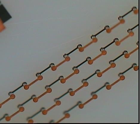
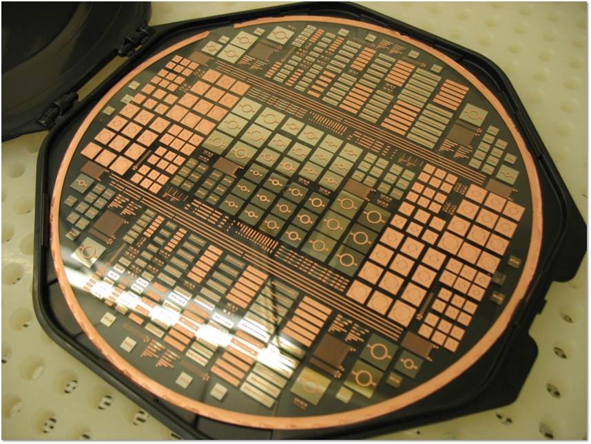
Through Glass Vias (TGV) formation allows to use glass as substrate for 3D integration for applications like RF modules and sensor packaging. Fraunhofer IZM has developed a TGV Cu- ECD process to generate hermetic filled Vias as low cost process without CMP and grinding steps. All processes are carried out using leading-edge, industry-compatible process equipment for 200/300 mm wafers.
Glass is well established as wafer or panel substrate for applications like capping of image sensors or as low loss carrier for integrated passive devices. Glass substrates with higher functionality becomes more attractive for the advanced packaging due the improvement of glass processing and the increased implementation of photonic packaging which is demanded for higher data transfer rates. The smooth surface allows the realization of ultra-fine wiring. Also, due to its transparent characteristic, it is well suited for the assembly of photonic components.
The usage of glass for applications like high density interposer is significant enabled by the improvements of the forming process of vias into the glass by laser drilling, electrical discharge or alternative technologies.
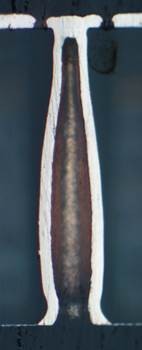
The technology allows to generate small glass vias with high aspect ratio and low pitch.
Technological competencies
- Via diameter down to 50 µm in a 300 µm thick glass substrate
- Low stress conformal via metallization
- Metallization by SAP with a high aspect ratio seed layer sputtering or electroless copper metallization by Atotech
- Hermetical via metallization (helium leakage tested)