The vertical arrangement of system components like logic- or memory chips as well as ASICs or sensors represents an efficient method for the volume reduction of systems but also for improvement of the systems electrical performance.
To enable vertical system architectures the particular ICs have to be equipped with vertical Though Silicon Vias (TSVs), which enable routing of electrical signals from the ICs front side to their backside.
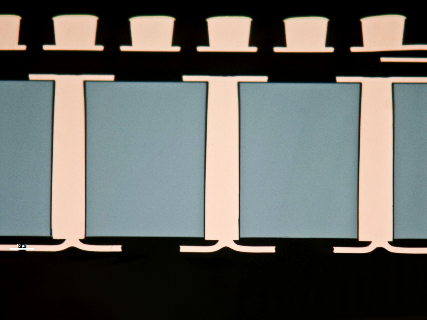
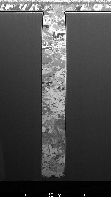
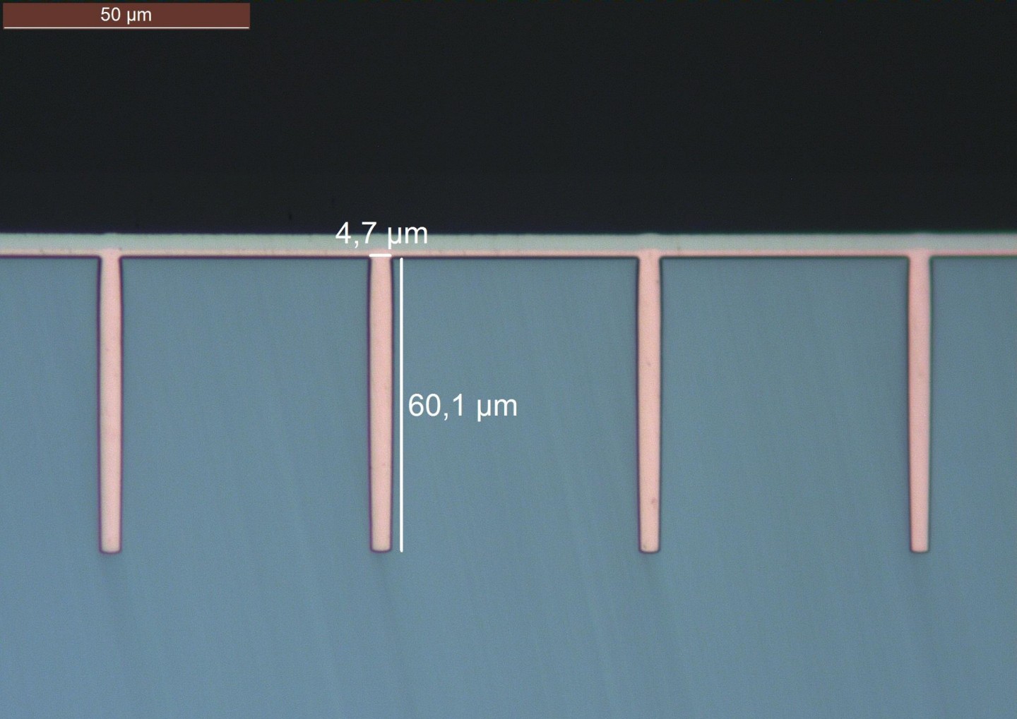
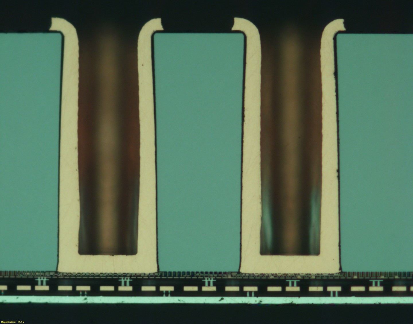
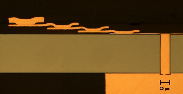
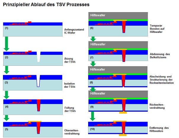
The fabrication of such structures is highly custom- and application specific and is established at 200 mm and 300 mm wafer level process equipment. In first steps of the fabrication flow, small holes are etched from the front side into the IC wafer until a certain depth is reached. Following the blind holes are isolated and subsequently filled up with copper as conductive material. In further processes, routing layers and contact structures are deposited at the wafer top side. Due to a subsequent thinning of the wafer from the backside, the copper plugs are revealed and can be connected and redistributed by further wiring layers. Finally, according to the assembly concept of the created device, contact structures are deposited at the wafer backside. All required structuring processes are defined by lithography, which provides a high degree of flexibility in fabrication of both TSVs as well as routing and contact structures.
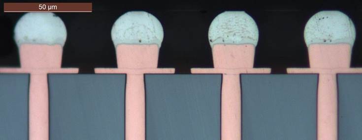
The described process flow is also used for the fabrication of TSVs into passive silicon wafers to create silicon interposers. Such interposers are mainly used as adapter between the high density IOs of integrated circuits like processors or memories and organic carriers, which only feature larger IO geometries. The interposers act as carrier devices onto which the ICs are assembled and interconnected via high density routing layers provided by the interposers. Signals, which have to be directed to the next system level, are routed via the TSVs onto the backside of the interposer where larger contact structures enable a proper assembly of the module to organic carriers.