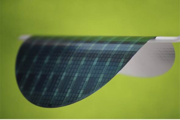
The fabrication of ultra flat devices and stacked system architectures is becoming more important ever. In this context technologies for extreme wafer thinning, thin wafer handling and thin wafer backside processing are imperative to enable 3-dimensional system architectures based on through silicon vias (TSVs).
Fraunhofer IZM is focusing its research on temporary wafer support systems based on adhesive wafer to wafer bonding of product and carrier wafers. With this approach, wafers can be thinned and handled without the necessity of adaptions on existing tools and process steps. Such systems enable wafer thinning as well as reliable support of thin wafers during standard processes like CVD and PVD, lithography, wet and dry etching, electroplating and polymer curing as well as an easy de-bonding of the temporary support wafer from the device wafer after final processing including residue free adhesive removal.
Due to the special design of carrier wafers, adhesives and de-bonding equipment different release mechanisms are possible to finally separate both wafers from each other after the processing was finished. Basic methods are solvent or laser release without heat using special designed glass carrier wafers as well as zone bond or slide-off release at elevated temperatures. All methods have their particular pros and cons and are evaluated carefully also in correlation with the corresponding kind of customer wafer to be bonded and de-bonded with them.
Based on the configuration of the customer wafer (surface materials and topography, thickness, kind of processes to be applied) as well as the subsequent sample treatment like second level assembly of components, the most suitable handling concept and wafer support system can be chosen. Even the cascaded use of the same support system or the combination of different style temporary wafer handling systems is possible to enable thin wafer transfer bonding.
Technological competencies
- Extreme thinning and stress relief of silicon wafers with different type of front side topography
- Back side processing of thin wafers with different front side topography including isolation / passivation, high density redistribution, contact formation
- Multiple thin wafer transfer to enable alternated front and backside processing
- Chip to thin wafer assembly
- Temporary support of thin chips during assembly
- Stacking of thin components at wafer level and component level
- Temporary Bonding: device wafer thickness > 20 μm, solvent release, slide-off release, laser release
- Enhanced dicing technologies (dicing streets > 20 μm)