Glass is a perfect material for optical application due to its high transparency. In contrast to polymeric materials Glass is also very temperature stable, highly chemical inert and has a very low water permittivity. Glass is not only used at Fraunhofer IZM as a carrier (wafer) for multilayer wiring but also as a thin layer for passivation and isolation.
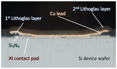
Through substrate vias in Glass (TGV, Through Glass Vias) is part of ongoing research activities. An additive microstructuring process is offered by Fraunhofer IZM in close cooperation with the company Lithoglas AG. Product examples are glass layers for photo-sensors, photo-diodes lowering substantially the packaging costs. In addition the layers are fully biocompatible which can be used or medical implantable devices. In contrast to existing glass structuring methods like sand blasting or etching this new method is based on plasma assisted glass e-beam evaporation in combination to a lift-off photo-resist process. Structures with a resolution of down to 2 µm can be achieved. The process temperature is below 120°C being compatible to organic and other temperature sensitive substrates.