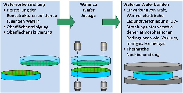
Permanent wafer to wafer bonding means the establishment of a durable joint between two wafers whereas the bond interface can be laterally structured or correspond to the full wafer area. The bonding can either be performed with functional intermediate layers as metals or adhesives or as direct bonding of the wafer surfaces without intermediate layers.
The available equipment offers the possibility to apply pressure, temperature, electrical voltage or UV light or a combination of them to the wafers to be bonded. Based on that anodic, eutectic or thermo compression based processes can be performed in vacuum, formic or inert atmosphere or ambient air. The required bonding materials like metals or adhesive layers like polymers, epoxies or acrylates are deposited in separate steps prior to the bonding process.
A special tooling allows transferring glue from a “help wafer” to topography features like frame structures of a device wafer, if for some special reason dedicated surface areas of the device wafer must not be coated with adhesive. In order to gain defect free, stable and reliable bond interfaces all over the entire wafer surface pre-treatments as particle removal, wet chemical removal of residues as well as surface activation by plasma can be done.
The wafer to wafer alignment is done prior to the bonding process by using suitable marks, which are located at the front sides or at the front and back side of the wafers. By utilizing optical microscopes and precise positioning stages the wafers can be aligned with an accuracy of a few micrometers. All processes are run recipe controlled at fully- of semi- automated production equipment.