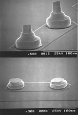
Platinum as Under Bump Metallization (UBM): With a modified wire bonding machine Platinum stud bumps are formed directly on the Aluminum pads (see figure 1a). After flattening (figure 1b) these bumps are suitable as UBM to provide a solderable, smooth surface and to act as a diffusion barrier between solder and Aluminum. For eutectic PbSn bumping solder balls or solder stud bumps are available. In the reflow step the solder is wetting the whole Pt stud bump forming a ball which incorporates the Platinum as a hard core (figure 1c).
Palladium is available as material for such a mechanically bumped UBM, too. However, compared to Platinum the reliability is rather weak due to the formation of Pd-Sn intermetallic phases. Nevertheless the Palladium UBM can be used for prototyping and demonstrators.