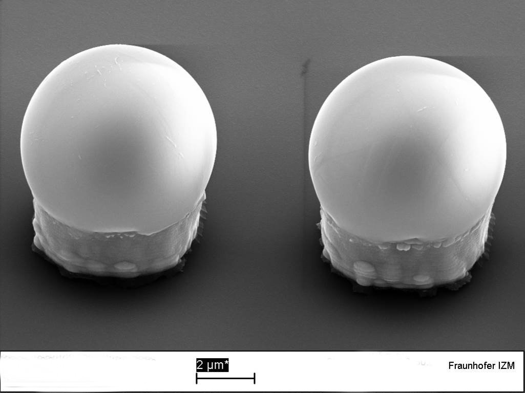
Solder bumps for flip chip assembly are deposited be electroplating on the I/O pads of the chips. The basic process steps of wafer bumping are sputtering of a seed layer (UBM), photolithography, electroplating of bump metal, etching of seedlayer and reflow.
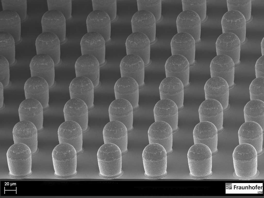
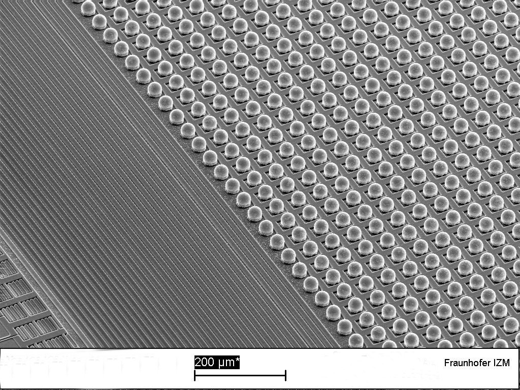
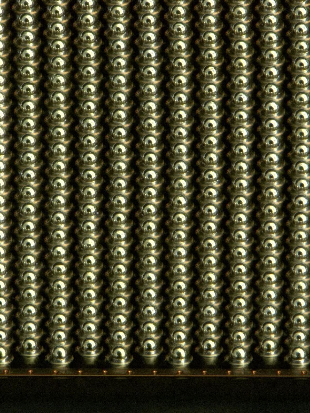
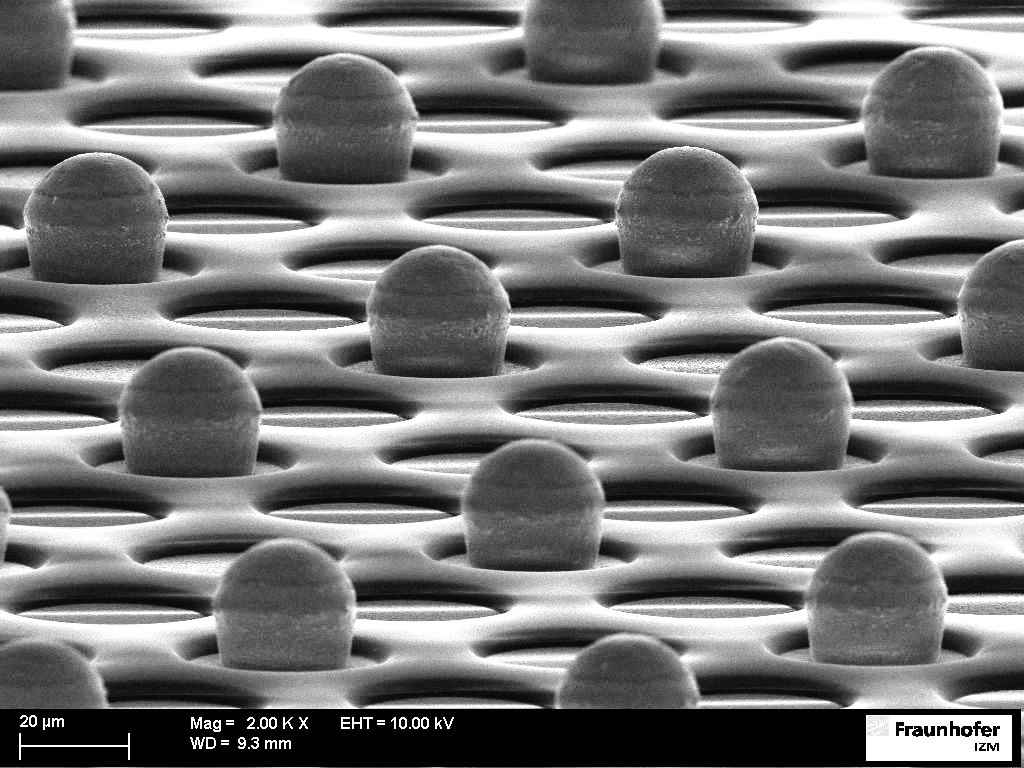
Bump structures of Au, Cu, Ni, SnAg, SnCu, SnAu with a dimension of min. 20 µm and with a pitch of 40 µm and height variation of less than <2 µm (8“) for bumps (25 µm height can be realized by electroplating.
Wafer of different materials (Si, GaAs, glass etc.) and with different sizes (4“-8“) and a thickness of about 150 µm (4“) – 650 µm (8“) can be used for bump process. After bumping the wafer can be thinned according to the specific requirements. An optional full wafer optical inspection provides a bump yield determination (wafer map).
Wafer with the formats 100 mm, 150mm, 200mm and 300 mm can be processed. On request, the processing of special wafer sizes and already singulated chips can be realized. The fabrication of microbumps by electroplating can be done on all common wafer materials (Si, GaAs, Glass, inP, Ge, etc.) with various passivations (SiOx, SiNx, Polyimid, BCB, etc.).