Further cost reduction, performance increase and miniaturization of electronic systems requires new highly efficient SiP concepts for MEMS components like RF resonators or switches, quartz crystals, bolometers, BAWs etc.
The usage of wafer scale bonding processes of cap structures for simultanious sealing of devices on the target wafer is a promising approach to evolve the next package generation for such components.
Capabilities and Research Focus
Fraunhofer IZM offers a versatile technology approach to serve such wafer level MEMS packaging concepts.
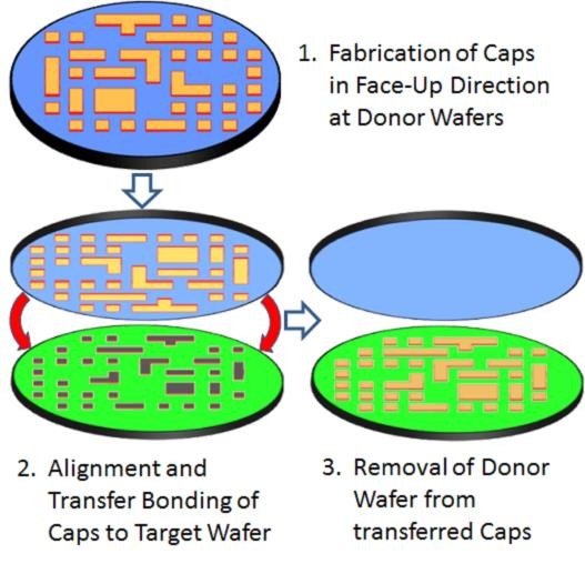
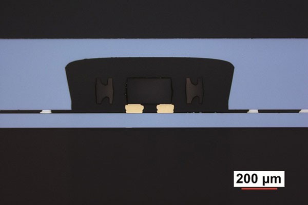
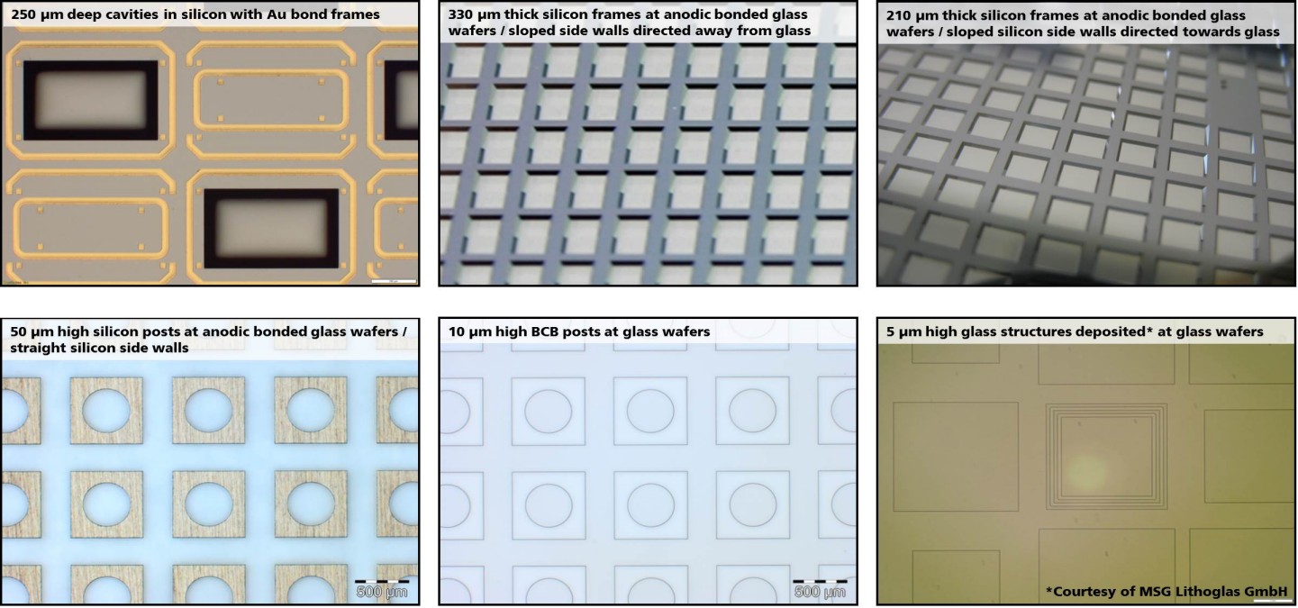
Basic idea of the wafer level capping technology is based on cap structure fabrication on a compound wafer consisting of two temporary bonded wafers. One wafer acts as carrier wafer whereas the other wafer is treated by processes like silicon thinning, silicon dry etching, deposition and structuring of polymer or metal bonding frames and optional partial pre-dicing to form arbitrary shaped and separated cap structures. Thus, the fabrication sequence transforms the original compound wafer into a carrier wafer with singulated, face-up mounted cap structures. The size, form, location and pitch of the cap structures matches with the devices on the corresponding target wafer, where the caps will be bonded to.
The so prepared cap donor wafer is now used in a wafer to wafer bonding process to align and bond all cap structures in parallel onto the desired positions at the target wafer. The wafer bonding process utillizes heat, pressure and defined vacuum conditions to permanently bond the seal frames of the caps with the surface of the device wafer. Since temperatures up to 320 °C can be applied with the current process flow, eigther adhesives but also solders/alloys like AgSn, CuSn, AuSn for hermetic sealing can be used as seal ring materal.
After the cap structures are permanently bonded to the device wafer, the temporary carrier wafer is removed from their backside. Remaining glue at the back side of the cap structures is removed by dry or wet cleaning methods.
Technological Competencies
- Quasi-hermetic capping by adhesive bonding
- Hermetic capping by soldering or metal-metal bonding
Due to the mask defined fabrication of the caps out of the compound wafer, a fully custom specific selective wafer level capping is possible with irregular areas and locations to be capped on the target wafer.