Key Research Areas

Packaging for high-frequency integrated circuits

Aufbau- und Verbindungstechnik für die Hochfrequenzsysteme / High-frequency packaging
© Fraunhofer IZM

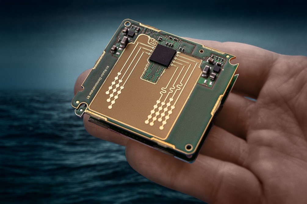
Packaging of communication modules comprises a multitude of technologies. Due to rising operation frequencies the impact of interconnects to signal amplitude and integrity becomes more relevant. We develop, analyze and optimize all connections in a package with respect to the technology for the development of new productions processes as well as for the production of state-of-the-art modules. We have a deep understanding of various process steps and their effects on signal integrity to optimize circuit layouts accordingly.

The spectrum of applications is huge and grows. It covers well known applications in wireless communication, e.g. base stations for 4G, 5G and upcoming 6G mobile networks up to specialized satellite communications system, such as LEO, MEO and GEO (terrestrial and space elements). Beyond that a multitude of radar sensor applications become more important, such as autonomous driving, e.g. tracking of trains, buses and other vehicles to optimize traffic and to avoid accidents) and home or consumer applications, (e.g. detection of persons and for home device control).


Working Group

Communication Module Development

The Communication Module Development Group explores how materials interact with high-frequency waves, including established packaging materials like conventional circuit boards and extending to other materials not primarily meant for packaging, but used in the automotive or communication sectors.


Working Group

Assembly and Encapsulation

We research integration technologies for system-in-package products, focusing in particular on device assembly for highly integrated packages and joining/encapsulation processes based on polymeric materials. Our technology portfolio includes pick-and-place processes – also for large-area substrates and 3D assemblies – and a wide variety of encapsulation processes, from dispensing and jetting to transfer and compression molding.


Key Research Areas

6G packaging

While the microelectronic market is more and more shifting to 5G and mmWave 5G, the research community is already working on the 6th generation of mobile communication. A final network architecture for the new generation has not yet been defined.  


Department

Wafer Level System Integration

The department "Wafer Level System Integration" (WLSI) develops advanced packaging and system integration technologies and offers customer-specific solutions for microelectronic products in the overall scope of smart system integration.