Low Inductance
Siliconcarbide semiconductors provide a high current slope during turn-on and turn-off. This can be used for a significant increase in switching frequency. Switching losses can be reduced, but at the same time overvoltages during turn-off, which occur due to the inevitable parasitic package inductances, become more considerable. They can destroy the chip and lead to further ringing which force up switching losses.
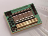
In the project presented here, two modules are built up and compared to each other: one conventional style, with wire bonds for chip contacts and broad busbars to connect the dc-link, and one embedded module. For the latter, chips are soldered onto a DCB in a standard process, but the dc-link is connected via a busbar realized in PCB technology. The DCB guarantees a much better thermal performance than a polymer.
Part of the dc-link capacitors is situated on the module.
A current slope of up to 4A/ns and only little overvoltage and ringing during turn-off can be achieved that way. Commutational inductance is only 0.866nH.
Commercial available current measurement systems could not provide accurate switching-current measurement, an inductive shunt was developed to characterize the module.