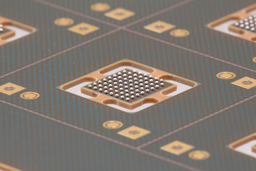
Balling for SiP / balling for interposer
Today’s packages with their high I/O counts call for high density interconnect schemes, typically a ball grid array configuration for SMT compatible mounting is used. Balling processes are also applied for Chiplet interposers, fan-in and fan-out wafer-level packages and for single die bumping. For the balling process solder preforms of different diameters (> 80 µm) and different alloys (SnAgCu, SnBi, Cu-core, …) are used.
Various process options exist for solder ball application to panels, wafers, single modules. For single dies, for single SiPs or interposers as well as for repair a solder ball jetter of PacTech (SB²-Jet) is available, that allows single ball placement with integrated reflow (Ball Jetting) or ball placement into a flux or solder paste depot with subsequent reflow (Ball Drop). Ball drop processes are also available using Pick and Place equipment, allowing for cost effective balling of single modules with larger ball sizes (from d=400 µm).
For wafer and panel level balling, Wagenbrett equipment is available that allows the placement of solder preforms from 250 µm diameter. Here a stencil-based approach is used for cost effective processing of larger substrates.
Balling processes are a crucial technology block for microelectronics packaging including prototyping in advanced packaging and will play a key role for future activities as Chiplet packaging for automotive and industrial applications.
 Fraunhofer Institute for Reliability and Microintegration IZM