Failure Analysis COB
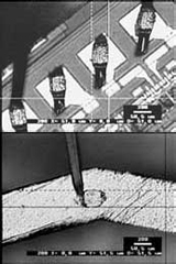
Cracks and voids in the glob top encapsulation of COB-modules
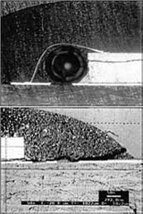
Board and chip interface heel crack
Typical procedures, especially for die- and wire-bonded as well as encapsulated semiconductor COB assemblies, are:
- Metallographic microsection preparation
- Decapsulation of encapsulation materials by plasma or HNO3 etching
- Light or scanning electron microscopic examination
Some results of such techniques are shown in the following illustrations. Of course, various other analytical techniques and possibilities for the characterisation of material and surface properties are available.