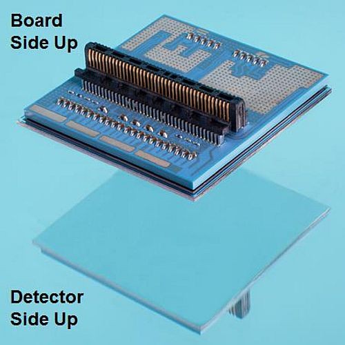
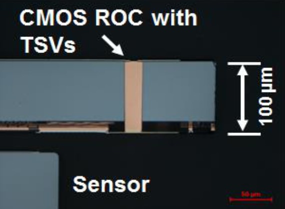
Fraunhofer IZM in Berlin and AGH University of Science and Technology in Krakow have developed 3D hybrid pixel detector modules for X-ray imaging. Each module consists of a silicon photon sensor die, two CMOS read out chips (ROCs) and one LTCC system board hosting periperal components. The sensor die includes 65536 single diodes aranged in a 256 x 256 matrix with a pitch of 75 μm. As ROCs two UFXC32k (Ultra Fast X-ray Chip with 32k channels) fabricated in TSMC 130 nm technology providing 128 x 256 IOs are monted side by side onto each sensor die to connect all of its 65536 individual photo diodes. As special feature through silicon vias (TSVs) in the ROCs enable a vertical routing of their 87 peripheral IOs to their back side where they are spread to a land grind array (LGA) with 800 μm pitch. Thus, the back side of the ROCs was used for next level interconnection to LTCC system board which allows a pure vertical system architecture. With this routing concept, area-consuming wire bond connections from the peripheral IOs of the ROCs to the system board are avoided which is the base for edgeless detector configurations with a tiled assembly of ROCs without imaging dead zones.
The system components of the 3D pixel detector modules were designed at AGH University of Science and Technology and the system packaging and assembly was done at Fraunhofer IZM in Berlin. The packaging tasks included TSV processing, front and back side redistribution and micro bumping of the CMOS ROC wafers as well as deposition of flip chip pads on the sensor wafers followed by wafer singulation and assembly of the modules. The 3D modules were built in a three-phase assembly process using high density flip chip assembly of the read out chips to the sensors, SMD assembly and balling of the LTCC boards and final flip chip assembly of the sensor sub-modules to the LTCC boards.
Final characterization of the fabricated detector modules using a dedicated evaluation board revealed good electrical performance. Test for power consumption and data communication performed within normal parameters. The modules were also run in real X-ray imaging experiments using an 8keV X-ray source. High resolution pictures with only max. 17 faulty pixels out of 65536 total pixels were taken which shows the good interconnect yield and the general capability of the chosen post processing and assembly flow.
Ref:
K. Zoschke et al., “Fabrication of 3D Hybrid Pixel Detector Modules based on TSV Processing and Advanced Flip Chip Assembly of Thin Read Out Chips”, 67th ECTC2017, May 30th – June 2nd, 2017, Orlando USA | more info