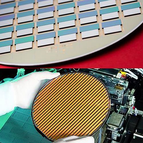
Besides wafer level post processing of semiconductor wafers including TSV integration, redistribution layers and fine-pitch bumping, Fraunhofer IZM has also long term experience in assembly technologies. As part of the department Wafer Level System Integration (WLSI) Chip to Wafer (C2W) assembly technologies offer a broad variety of processes to enable high density microelectronic packaging. One of the major advantages of (C2W) assembly relies on the fact that it offers principally a higher throughput compared to chip-to-chip assembly.
For carrying out wafer level assembly, singulated dies can be directly picked from dicing tape on frame after dicing or from waffle packs. Using mapping files and programming procedures (teaching of chip device and target substrate), Known Good Dies (KGD) or best-in-class dies can be selected and picked from the singulated chip wafer on dicing tape and subsequent- ly assembled on the desired positions of the target wafer. A recognition system allows the matching of the picked-up chip with its final position on the substrate wafer. If required, the picked dices can also be sorted in waffle packs.
Substrate and chip wafer up to 300 mm size can be assembled with flip-chip bonders of industrial ranks with different postbonding precision, the most accurate of newest generation achieving a postbond accuracy in the range of 1 μm. Substrate wafers can be thin silicon or glass interposer with TSVs on carrier or full thickness active wafers (CMOS). Chip thicknesses down to 50 μm can be usually operated on automatic bonders. Different assembly processes are basically possible using flip-chip or die attach, from thermode bonding, as well as pick-and-place followed by flux-free batch reflow and even up to wafer bonding by means of reconfigurated wafer. Here, Known Good Die are first temporary bonded on a common temporary carrier wafer (recon- figuration) by means of a temperature resistant adhesive and then simultaneously bonded to their common target wafer substrate.
Thermocompression bonding (Au, In) and soldering (Cu/Sn, SnAg, Au/Sn based) are the most representative interconnecting processes allowing heterogneous integration. Not only single die but also multiple die can be assembled on a same target substrate, enabling the fabrication of System-in-Package (SiP). All assembly processes are carried out in clean room environment of class ISO 6 (i.e. 1000 FS209) with care on ESD safety (floor, equipment, persons).
 Fraunhofer Institute for Reliability and Microintegration IZM