Fraunhofer IZM offers a variety of processes for the manufacturing of flexible or rigid / flexible high density multi-layer circuits. The fabrication approach features the capabilities of the well establisted wafer level redistribution technology, which is applied on temporary carrier wafers. The high density wiring layers are generated in semi-additive technology using electro-plated copper or gold. Typical is a metallization height of up to 5 μm and line pitches down to 20 μm. The inter dielectric layers with micro vias are fabricated by spin coating, lithographic structuring and cure of photo sensitive polyimide precursors. A multi-layer build up is obatined by sequential alternated processing of polyimide and metall layers. So far, with the current technology, fully flexible interposer curcuits with up to four internal metal routing layers were fabricated, which had a total thickness of approx. 50 μm. The technology also allows the embedding of thin ICs or sensor components inside such flex circuits. To enable that, approx. 20 μm thin devices are die bonded onto one of the initial polymer layers. A following overcoating with polymer completely covers the thin devices. Their IOs are accessed by lithographic structuring of vias into the photo sensitive polymer layer. The electrical connections to the IOs are then established by the following wiring layer.
As further feature, vertical electrical conatcts through the flex substrates can be realized. With that option interconnections from the bottom to the top side of the flexcircuits become possible. A broad variety of pad metallizations like Cu, Au, NiAu, or solder enable different assembly processes for the flex cirquits.
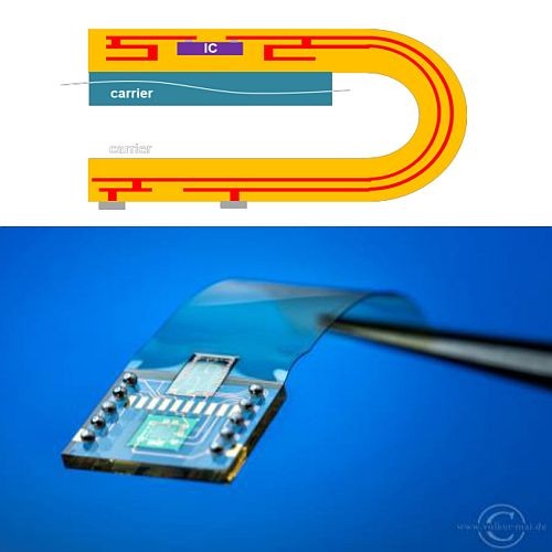
After the complete processing of the multi-layer build up it will be detached from the temporary carrier wafer using a special designed high speed de-bonding process. As special feature, the technology allows also the only partial release of the carrier substrate in dedicated areas. By doing so, rigid and flexible zones can be created within one circuit to serve certain functional or mechnanical requirements. The upper image shows a schematic drawing of a rigid / flex with an embedded IC in the rigid part as one exemplary implementation option of the technology. The bottom image shows a sensor module, which was fabricated in rigid / flex technology. It hosts two only 20 μm thin embedded devices for stress and vibration detection and can be used for condition monitoring and observation of sensitive equipment. The flex build-up with the embedded devices has a thickness of approx. 50 μm. To gain maximum inertial sensitivity the vibration sensing device is located at the transition between flexible and rigid part.