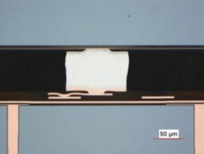
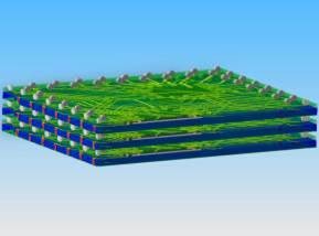
Silicon and glass interposers offer new possibilities to merge advanced devices e.g. high pin count ASICs, memories and MEMS to form 3D SiPs. Depending on the product requirements they can be realized fully customer-specific with a high degree of flexibility in lateral size, TSV/TGV geometry and density as well as number of routing layers and nature of IO terminal pads for component and second level assembly.
Silicon Interposers with vertical through contacts act as component carriers or adapters between integrated circuits with highest IO densities and organic carrier. They are created with established TSV middle or TSV last processes. Current TSV generations also include integrated active devices and will be optimized for high power dissipation and high speed data transmission. Glass interposer especially bear advantages in specific silicon/glass packages and also in large area substrate applications.