Fraunhofer Institute for Reliability and Microintegration IZM
Workshop / October 17, 2018
Wafer Level Packaging & Sensor Integration
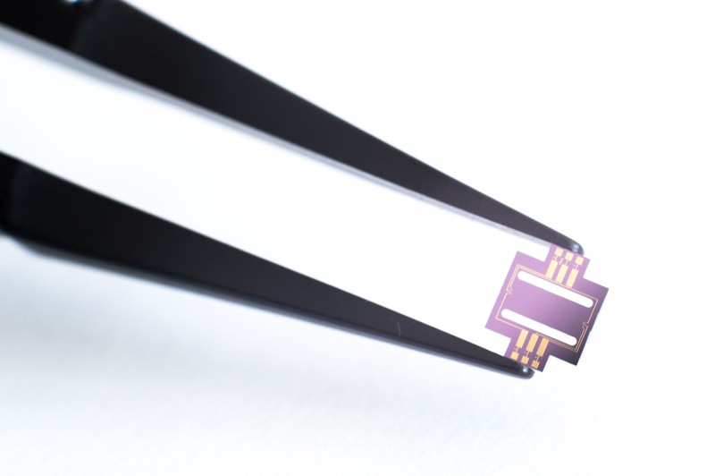
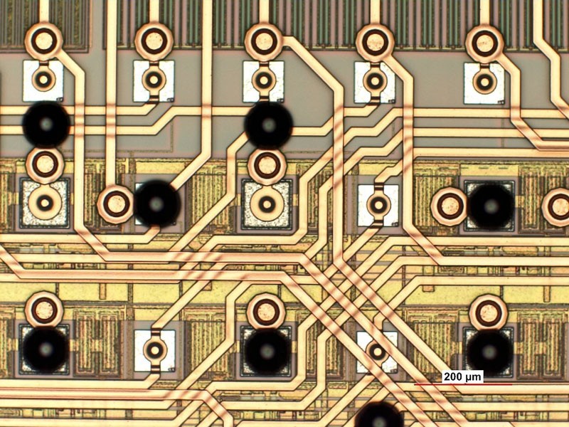
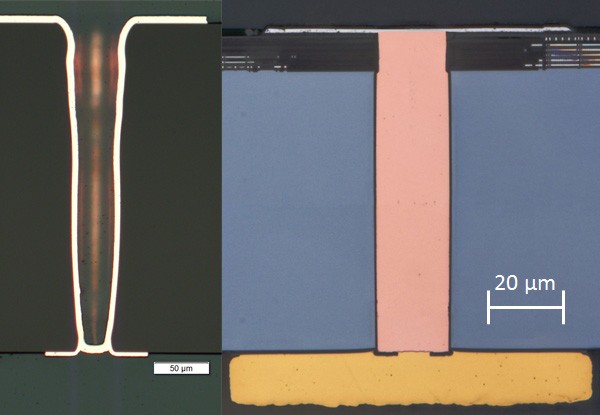
Wafer level packaging is a synonym for the whole technology spectrum enabling direct chip attachment on PWB or other substrates by flip chip interconnection. In contrast to pure bumping processes additional thin film wiring layers are required featuring a higher level of integration by embedding active or passive devices onto the chip. The technology is feasible for any kind of CMOS wafers but also for III/V or even sensors.
Contents
- Wafer bumping and multi-layer metallization
- Fan-in / fan-out wafer level packaging
- 2.5D / 3D Integration technologies
- MEMS and sensor packaging
- Wafer level capping and wafer bonding
- Assembly technologies (chip to chip, chip to wafer, chip/ module to substrate)
- Realization and integration of sensors and sensor elements
- Analysis and measurements methods