Focus on cybersecurity: Researchers develop photonic encryptions
Cybercrime incidents are on the rise: To protect information in electronic components from tampering or illicit use, a crack consortium of research institutes, private enterprises, and universities have formed the »Silhouette« project to develop solutions for encrypting data in the optical domain that is considered safe from tampering and eavesdropping. Researchers at Fraunhofer IZM are part of this campaign and are developing a cost-efficient method for the precise coupling of microelectronic components to make data transmissions safer and more secure.
The digital evolution is showing its dark side: Cyberattacks have become common, and more and more enterprises and private individuals are falling prey to them. Protecting sensitive data, especially in open processes, needs reliable electronics, whose development the German Ministry of Education and Research is funding with its “Trustworthy Electronics” campaign. One solution that is attracting increasing attention here is the use of optical transmission, which is considered much safer from wiretapping and promises much faster speeds in operation.
In their quest to transmit sensitive information by photonic signals, the research consortium behind the »Silhouette« project is working on a modular standardized platform with an electro-optical interposer as the interface turning electronic into optical signals, transmitting it to its intended recipient, validating it, and translating it back into electronic signals. The experts on the project are committed to making this novel process compatible with current hardware solutions as a key step towards new hybrid systems for future cryptography.
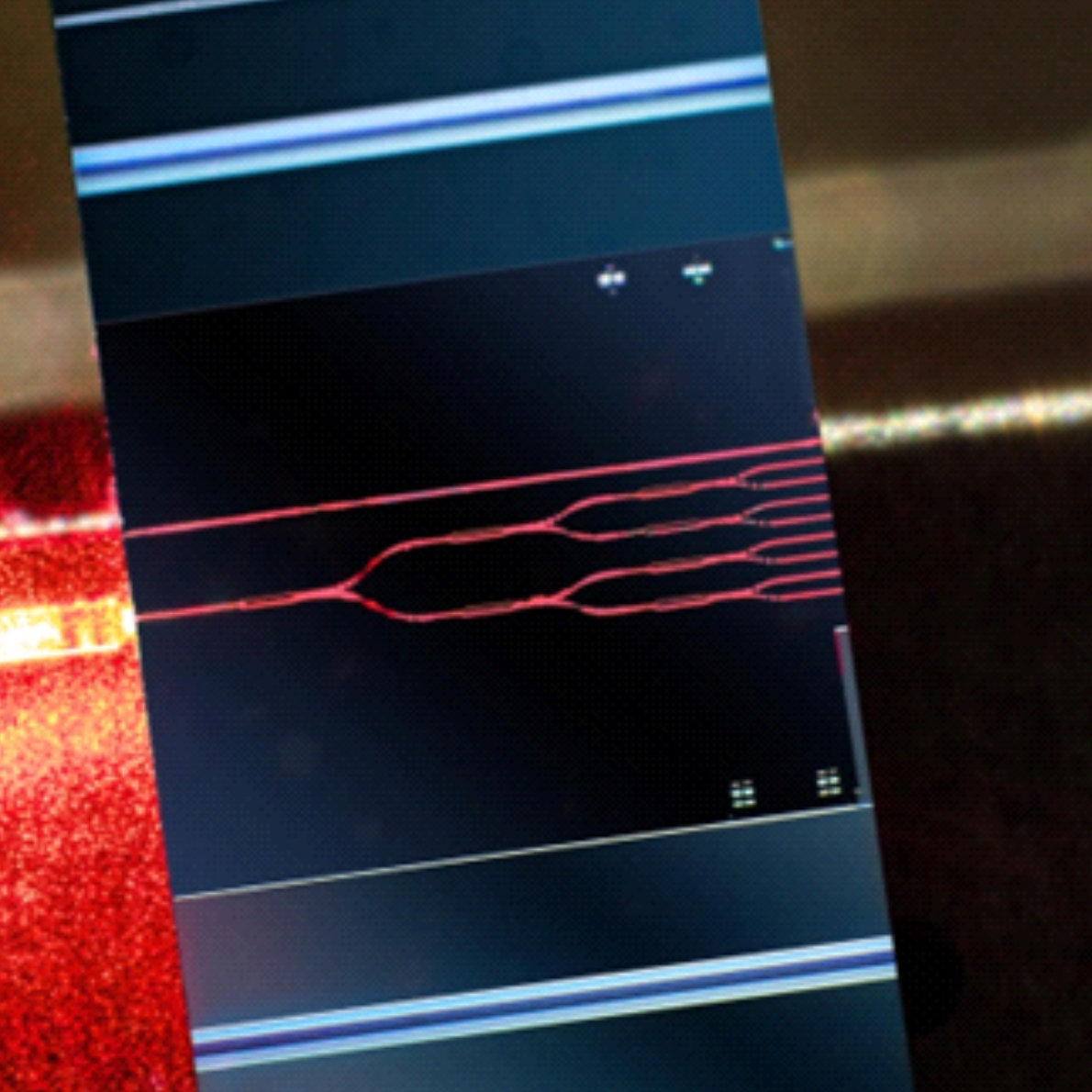
The team assembled by Dr Hermann Oppermann at Fraunhofer IZM is responsible for developing and integrating the microelectronic and opto-electronic components of the interposer. They chose optical waveguides to channel the light signals, which guarantee far more efficient transmissions when compared to conventional lenses or mirrors. The cost of this added efficiency is the extreme precision it needs when coupling the waveguides to achieve lossless transmissions and to make it a viable medium for calculations with the optical data package. It is this extremely fine connection that is proving a challenge in practical terms: “The waveguides used on the optical ICs are extremely tiny with a diameter of less than one micrometer. When you get to such tiny dimensions, any active alignment of the components would be far too costly and labor intensive. That is why we are developing passive options as an alternative, which means that the photonic circuits could be mass produced at lower cost, which makes them a real choice even for smaller enterprises”, Dr Oppermann explains.
His team managed the extremely precise self-alignment of the components with special indents or cavities in the interposer: The cavities measure around ten micrometers and provide a type of mechanical stop in the system. Solder bumps are placed in each cavity to help navigate the delicate structures softly and carefully into their target position. When the solder is melted, it catches the laser diodes of the integrated waveguides and pulls them into place by simple surface tension. First tests show that this solder-driven self-alignment managed to move several hundred diodes into their target location in one go. Used in industrial production, this parallel mass reflow of laser diodes could lower the production costs for the interposers by five percent.
In a first step, the designs of the individual components are carefully aligned with each other, and the necessary electrical connections developed. Before the project’s scheduled conclusion in 2024, all components and solder bumps must be prepared, the demonstrator model assembled, and the coupling efficiency tested and known for the entire system. First indications suggest that the integration of an interposer in the key generators and analog multipliers represents a major leap forward for encrypted communication and, by implication, more reliable data security.
The »Silhouette« project has a budget of €15 million to work with, of which €12 million were provided by funding from Germany’s Ministry of Education and Research. The project consortium includes several research institutes: The Fraunhofer Institute for Photonic Microsystems IPMS (Dresden) as coordinator, the Fraunhofer Institute for Reliability and Microintegration IZM (Berlin) represented by its IZM-ASSID unit from Moritzburg, the Fraunhofer Institute for Telecommunications, Heinrich Hertz Institute HHI (Berlin), the Institute of Electronic Packaging Technology (IAVT) and the Integrated Photonic Devices (IPD) Group of the Technical University of Dresden, the tech R&D and manufacturer OSRAM Opto Semiconductors of Regensburg and the quantum optics developer and distributor qutools of Munich. The research work will progress until 2024.
(Text: Olga Putsykina)

Last modified:
