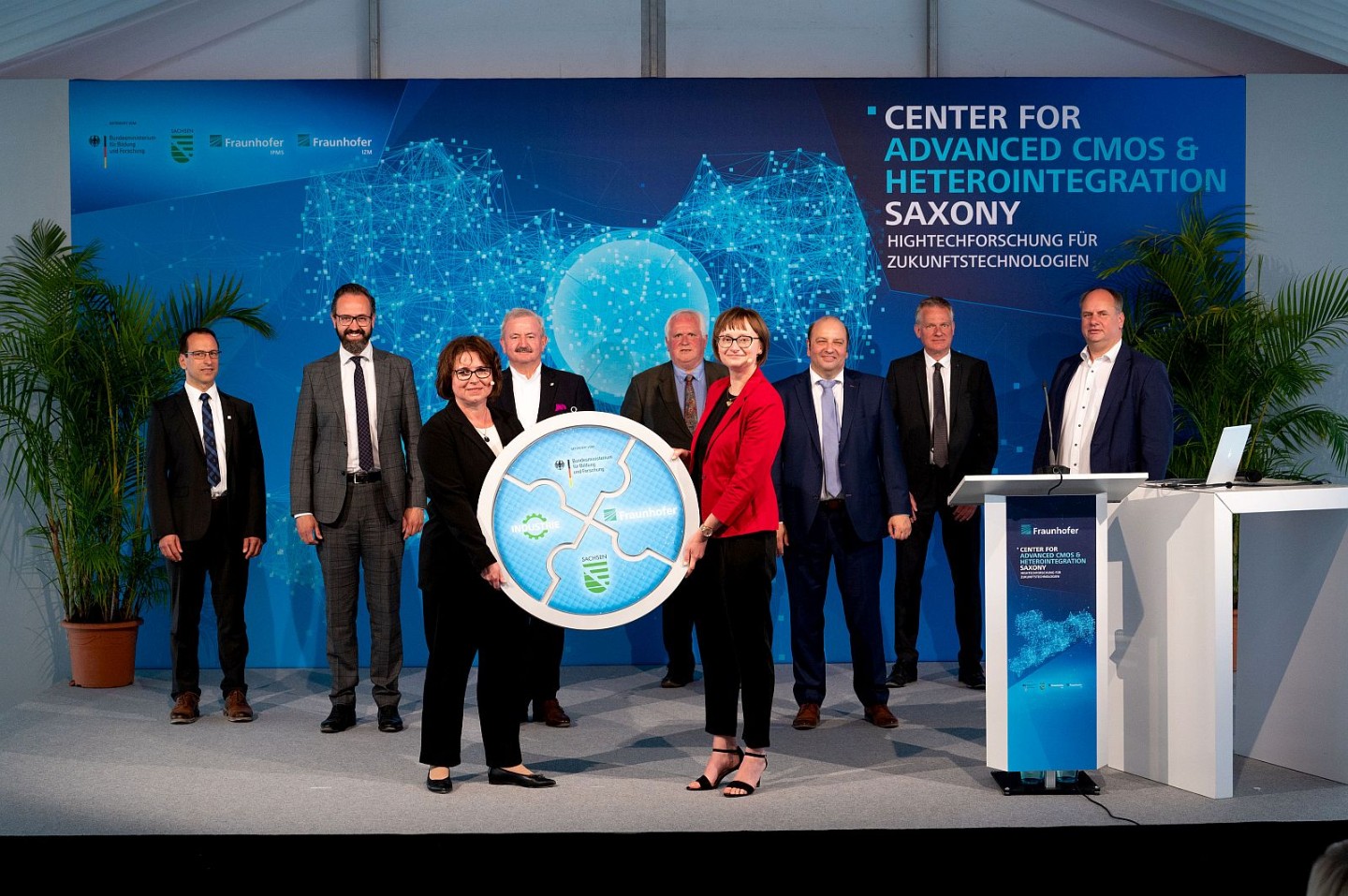
Ceremonial opening of the joint research center for 300 mm microelectronics of Fraunhofer IPMS and Fraunhofer IZM-ASSID
New center for semiconductor research opened in Dresden
A flagship of semiconductor research with international reach is emerging in Dresden. Fraunhofer IPMS and Fraunhofer IZM-ASSID are bundling their competences and establishing the Center for Advanced CMOS & Heterointegration Saxony. The center will offer the complete value chain in 300 mm microelectronics, a prerequisite for high-tech research for future technologies.

With Fraunhofer IZM-ASSID and Fraunhofer IPMS’ Center Nanoelectronic Technologies CNT, two unique research facilities in Germany in the field of microelectronics are located in Saxony. Today, they are the only two German research centers for applied microelectronics research based on 300 mm wafer industry standard equipment. With the bundling of competences and the foundation of the Center for Advanced CMOS & Heterointegration Saxony, excellent perspectives arise to attract semiconductor companies and system users as well as material and equipment manufacturers worldwide. In addition to excellent personnel and know-how, equipment with a modern equipment and plant park is crucial for industrial and research contracts.
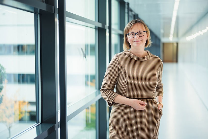
With an investment volume of about €140 million in clean room facilities, Fraunhofer IPMS is uniquely positioned in Germany in the field of applied research on the modern 300 mm wafer industry standard in the front end of CMOS manufacturing. Fraunhofer IZM-ASSID complements this expertise with innovative packaging and system integration technologies. In the future, the center will be headed by Dr. Wenke Weinreich, division manager at CNT and deputy institute director of Fraunhofer IPMS, and Dr. Manuela Junghähnel, site manager at IZM-ASSID.
Investment in future technologies
"The joint center with a clean room of 4000 m² in size enables close cooperation and networking of the scientific and technical competencies of both research institutions. This creates an outstanding R&D technology platform as well as an increase in efficiency and completion of the value chain, which at the same time opens up new research fields," explains Dr. Manuela Junghähnel. Dr. Wenke Weinreich adds: "The 300 mm wafer industry standard is crucial, because it is the only way to ensure a fast transfer of research results to the semiconductor industry in Saxony, nationwide and also worldwide. On the other hand, this wafer standard is also a basic requirement for high-tech research for future technologies, such as neuromorphic and quantum computing."
Ceremonial opening
The Center for Advanced CMOS & Heterointegration Saxony is being built at one of Fraunhofer IPMS’ sites in Dresden in the new 4000 m² clean room and is being ceremonially opened today. Saxony's Prime Minister Michael Kretschmer: "Saxony is one of the leading microelectronics locations in Europe. Every third European chip is produced in the Free State of Saxony. With the European Chips Act, the EU has set the course for further investments. Saxony relies on close networking between industry, science and research. The new Fraunhofer Center for semiconductor research is unique in Germany and will make a decisive contribution to innovation in Silicon Saxony. In the future, applied microelectronics research with state-of-the-art 300mm wafers will take place in Dresden at world level. High-tech research for future technologies ensures innovative strength and prosperity in the Free State of Saxony. I thank the Fraunhofer-Gesellschaft for its clear commitment to Saxony as a location."
The President of the Fraunhofer-Gesellschaft, Prof. Dr. Reimund Neugebauer, is also impressed: "The new Center for Advanced CMOS & Heterointegration Saxony is an excellent example of proactive shaping of the European development of semiconductor technologies and makes an important contribution to securing our technological sovereignty. By bringing together excellent scientific and technical competencies, the center will efficiently map the entire value chain of semiconductor technologies in the future - from research and pilot production on 300 millimeter silicon wafers to contacting and final assembly."
For the future development of the necessary competencies in microelectronics and microsystems technology, the R&D offerings of Fraunhofer IZM-ASSID and Fraunhofer IPMS with regard to 300 mm process competencies will be designed and expanded in such a way that local and national industry from SMEs to large companies (e.g. Globalfoundries, Infineon, Bosch) will be able to benefit from the latest technologies in the best possible way. The integration platform is also used in customer-specific projects as part of the High-Performance Center "Functional Integration in Micro- and Nanoelectronics" performance center and in the Research Fab Microelectronics Germany (FMD).
With a positive view of this network, Saxony's Minister of Science Sebastian Gemkow concludes: "For the future of microelectronics research and technology development in Dresden, Saxony, Germany and Europe, the opening of the CNT is a milestone. In a joint effort of the Fraunhofer-Gesellschaft, the federal government and the Free State of Saxony, we have succeeded in securing one of the leading research facilities in the field of 300mm technology for the long term. IPMS-CNT and IZM-ASSID focus on strategic and deepened cooperation within the Center for Advanced CMOS & Heterointegration. Thus, 'Silicon Saxony' will be further strengthened and will make important contributions to the processing of future topics in microelectronics in the future."
About the Center Nanoelectronic Technologies

The Center Nanoelectronic Technologies CNT is a business unit of the Fraunhofer Institute for Photonic Microsystems IPMS. It performs applied research on 300 mm wafers for microchip producers, suppliers, device manufacturers and R&D partners. For processing customer orders, 4000 m² of clean room space of class 6 and 3 (according to ISO 14644-1) as well as laboratory space for more than 80 processing and analytical tools are available. The equipment pool includes deposition and etching equipment as well as inspection and analysis equipment for determining defects and measuring layer properties.
About Fraunhofer IZM-ASSID

Fraunhofer IZM-ASSID, a branch of Fraunhofer IZM, has a state-of-the-art 200-300 mm technology line for 3D wafer-level system integration based on copper-through-silicon-via (Cu-TSV) technology. The process line at Fraunhofer IZM-ASSID is especially designed for production-oriented and industry-compatible development and processing (ISO 9001). Components of the line are process modules for TSV forming, for post-TSV processing, pre-assembly (thinning and separation), 3D stack forming. The conception of the line allows both an application-related development of processes and the qualification and prototype production for 3D wafer-level system in packages.

Last modified: