Online-Session / January 25, 2022, 16:00 - 16:45 CET
High density thin film flex - technology and applications
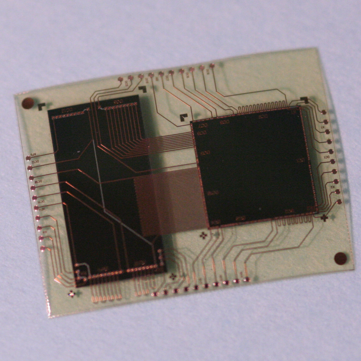
The presentation provides a latest technology review for fabrication of high density thin film flex and related application examples. The fabrication approach utilizes the well-established processes from wafer level packaging and redistribution technology. Multi-layer routing structures are built by sequential processing of polyimide and semi-additive metal on a carrier wafer with a dedicated release layer. Depending on the number of copper routing layers with typical thickness of 3-5µm and the required polymer inter dielectric thickness the final multi-layer stacks can have total thicknesses between 20-60µm. A laser assisted process allows an easy detach of the thin film flex circuits from the carrier wafer. The technology allows high density routing with line pitches <=12µm over all layers, custom specific front and back side contacts of Au, Cu, NiAu or solder (only front side) adapted to subsequent assembly technologies, embedding option for ultra-thin ICs, option for partial rigidness by utilizing the carrier as permanent stiffener as well as option for arbitrary shaped outlines. All details regarding the different implementation options will be discussed in the presentation.
Furthermore, possible application fields of the high density thin film flex technology and related examples will be discussed in this presentation. In many cases, the ultra-thin profile of the flex circuits with the feature for hosting embedded ICs is of great benefit for different types of sensor applications. Based on that, senor systems with embedded ICs for vibration monitoring or RADAR detection were fabricated for industry 4.0 related use cases.
Flex circuits can also be used to enable the wearability of electronics for example in healthcare or smart clothing application. One example from the European project APPLAUSE will be presented. One goal of that project is the development of a flexible medical patch for cardiac monitoring of patients. A thin film flex with embedded ICs will be the part with the highest integration density. The flex itself provides large IOs and will be embedded into stretchable polyurethane, which carries the remaining components of the sensor patch using low integration density.
As another aspect, flex circuits can be used as low profile polymeric interposers or stackable substrates. In that case, the flex circuits are designed with proper front and back side IOs, so that components can be mounted and the flex themselves be mounted on a further substrate. A very interesting approach is the stacking of flex layers in case that very high number of routing or redistribution layers are required. In that case, the flex circuits are assembled on top of each other to create a flex stack. Such a stack of flex circuits can be mechanically stabilized by liquid or pre-applied under filler. The 3D stacking approach enables multiple stacking of flex substrates resulting in a multiplication of the available high density routing layers. Especially for extreme routing requirements, this approach might be an alternative compared to sequential processing of all routing layers in one build-up, which suffers from technological limitations, longer lead time, higher cost and lower yield.
 Fraunhofer Institute for Reliability and Microintegration IZM
