Embedding

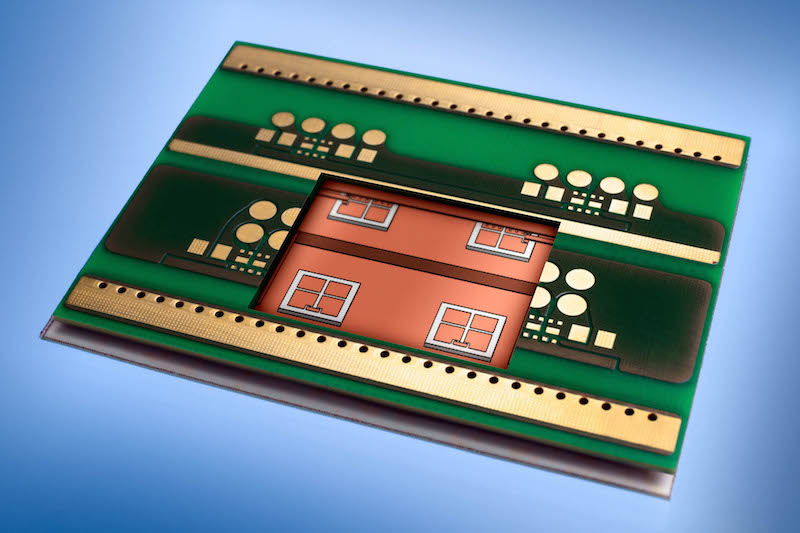
Embedding is the process of integrating components, often chips, in PCBs. Both active and passive components can be embedded in laminates. The process has many advantages over conventional packaging techniques.
More info:
Embedding makes thin, planar modules possible, which can then be stacked into 3D systems. It also allows developers to keep the inductivity between electrical connections to a minimum and provides for the integration of shielding layers. Using conventional PCB techniques, embedded components are directly interconnected through microvias and copper plating, providing excellent electrical properties and high reliability. The embedding techniques we use combine the advantages of conventional PCB manufacture with high-precision SMT component mounting. Component assembly can be divided into two main approaches: “Face down” – the chip is mounted with the bond pads facing downwards – similarly to flip chips – and “face up” – the semiconductor is mounted with the bond pads facing upwards, as in wire bonding assembly. The resulting package is similar, but the two techniques lend themselves to different applications.
Face-down assembly
In “face-down” assembly, the chip, with its bond pads facing downwards, is adhered to a thin, pre-patterned copper film using non-conductive adhesive. After applying resin-coated copper film (RCC) or prepreg, the chip is embedded by vacuum lamination. The components are then electrically interconnected through microvias. As in conventional PCB assembly, laser drilling, desmearing, through-hole activation and galvanic copper deposition can all be used to fashion the microvias. The conductive pattern is created by photolithographic patterning of the substrate’s copper layer, followed by etching. Finally, the substrates with the embedded chips can then be processed into multilayer build-ups just like conventional PCB inner layers. The “face-down” approach is already popular in series manufacturing and is particularly suited to components with small pitch.
Face-up assembly
In “face-up” assembly, which was developed by Fraunhofer IZM, the bottom side of the chip is mounted. The processing steps are identical to those in the “face-down” technique. However, the alignment of the chip in the PCB and, consequently, the interconnection, differs. Because the connection of the die by microvias is made through the embedding material, the base substrate is not limited to a copper foil. Other materials can be used, such as thick copper or pre-patterned inner layers. Furthermore, large-area bonding of the chip to the substrate is also possible using conductive materials, such as conductive adhesives, solder joints and sinter materials, instead of just non-conductive adhesive. The “face-up” technique is particularly suited to the embedding of vertical components, such as power MOSFETs, IGBTs and diodes.
Research and Development
Key research areas at Fraunhofer IZM include developing novel techniques for embedding electronic components in PCBs, investigating new basic and packaging materials and developing new processes for manufacturing HDI substrates. In detail, our current research focuses on:
- The investigation of new materials: analysis of basic materials with high glass transition temperatures (Tg) and low coefficients of thermal expansion
- The investigation of new materials forpower electronic applications: analysis of basic materials with high thermal conductivity and good electrical insulation
- Development of new materials for die attach: manufacture of thermally and electrically conductive interconnect materials such as silver sintering pastes, which can join materials at low temperatures without the application of pressure
- HDI patterning using semi-additive techniques: reduction of trace and pitch width from the current standard of 50 µm to 15 µm
- Interconnection of semiconductor chips: reduction of contact pitch from the current standard of 120 µm to a targeted 50 µm
- Module and housing designs for multilayer assemblies: development of embedded components with several layers for maximum miniaturization
Methods and Equipment
Fraunhofer IZM’s process development makes use of both destructive and non-destructive testing. Our technologies include light microscopy, scanning laser microscopy (SEM) and X-ray computed tomography (X-ray CT).
Microstructural analysis methods such as focused ion beam (FIB) are also available. The institute’s equipment also includes a flying probe tester (FPT) with 6 probes for detecting electrical failures.
Fraunhofer IZM helps technology and product developers:
- Select and qualify processing materials
- Design and manufacture customized prototypes
- Perform reliability testing on prototypes
- Implement process transfer
To provide these services, the institute has established a substrate technology line able to process substrates of up to 610 mm x 456 mm in single run. The processing line comprises the following individual steps:
- High-precision component placing
- Vacuum lamination pressing for manufacturing multilayer assemblies and embedding components
- UV laser drilling and patterning
- Mechanical drilling and milling
- Photolithographic patterning using laser direct imaging and dry film photo resist
- Horizontal spraying for HDI patterning
- Horizontal spray etching and photoresist stripping
- Automated and manual galvanic equipment
 Fraunhofer Institute for Reliability and Microintegration IZM