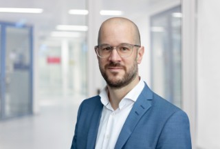
Fraunhofer IZM:
Mr. Schiffer, we are very excited to hear you summarize your 2019’s highlights and lowlights. But let’s start with you. On a scale of 1 to 10, how happy are you with the results achieved in your department?
Michael Schiffer:
I don't have to think about it for long. I’d give us a 9! I’m very happy with how my first year in this department went and I look forward to new successes in 2020.
IZM: The most important words have just been said, but let’s get down to the details. What were 2019’s successful projects and why?
MS: I can’t name a specific project, but I’m very excited about two developments that we achieved in 2019 and that we will continue to pursue. On the one hand, there are the new developments with companies where we’ve been able to reach structure size ranges of around one to three micrometers, thus reaching the technological vanguard in terms of resolution with our laser direct imagesetter. On the other hand, we were able to strengthen and expand our industrial services with partners we have worked with for years. These services include bumping for detectors in particle accelerators or sensor assemblies.
IZM: It certainly sounds as though there will be enough topics this year to keep you and the individual groups within your department busy. What topics will be included?
MS: Oh yes, I can’t see 2020 being any quieter than last year. I can see the following topics being of interest to us: For a start, within fan out wafer level packaging, the trend is towards ever smaller structures and higher numbers of layers, thus raising the question of the reliability of these kinds of packages and of which new materials could lead to an improvement.
There is also increased demand for the topic of heterogeneous integration in mold or silicon; particularly within the area of high frequency, where, together with the other departments at this location, we will develop innovative packages. The full bandwidth of the institute’s know-how is needed here.
Furthermore, wafer bond technology (whether permanent or temporary), offers manifold possibilities for 3D integration from hermetic packages to complete 3D systems, something that’s becoming more and more important in the area of chiplet technology, say.
IZM: But let’s be honest—sometimes there are bumps in the road. Even if you can’t or don’t want to go into detail about it, what do you hope runs more smoothly this year?
MS: In general, things are going pretty well at the moment. I have noticed, however, that—in addition to the package—an insight into the whole system is becoming more and more important, giving us an opportunity to expand the added-value chain. That is why we need to move more towards co-design of sensor elements and packages—with our sensor system group, for example—as this could result in new system approaches for future applications.
We also need to consider what test structures can be established in the packages in order to be able to determine specific properties (e.g. hermeticity, contact properties between different package levels, high-frequency properties, and the aging of dielectrics, etc.) through simple in-line measurements or random testing of packages. Here, again, it makes sense to look through your system glasses!
I continue to see a trend towards 300 mm wafers, where the aim is to close the odd gap in the process chain and to strengthen our cooperation with the Dresden site.
What's more, the administrative workload in project planning will probably increase and we will introduce a manufacturing execution system to increase the transparency of processes in the clean room. This needs universally applicable processes and ever closer coordination between the individual groups (and their members) along the process chain. One positive side effect is that the groups’ varying viewpoints allow us to come up with the best possible result in the end.
IZM: Last, but not least: If you could choose what your department stands for, what would you say?
MS: The existence of the complete process chain, from wafer oxidation to bumping—and, beyond that, to die assembly—the department can offer a wide range of facets but also the necessary technological depth. Our close relationship with industry allows me to see the department as the ideal partner when it comes to developing new, disruptive package technologies that we can look after right up to production handover.
THANK YOU VERY MUCH for giving us your time and for the many applied-research projects that you and your team are implementing.
 Fraunhofer Institute for Reliability and Microintegration IZM
