Online event | Expert Session Series / March 09, 2021, 4:00 pm - 4:45 pm
2.5D and 3D Wafer Level Packaging (Si/Glass interposer, 3DIC)
2.5/3D wafer level packaging is one of the important key technologies in advanced microelectronic packaging and system integration worldwide. This concept has specific advantages in terms of heterogeneous integration of multiple devices such as sensors, processors, memory ICs and transceivers with excellent electrical performance and small form factor.
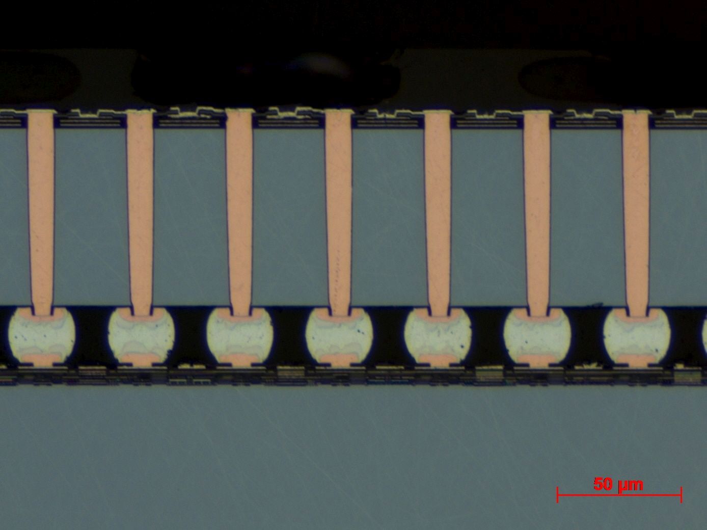
2.5D packaging approaches are based on passive silicon or glass interposers with through silicon vias (TSVs) or through glass vias (TGVs) which act as intermediate carrier to efficiently link several sub-components with excellent electrical connections together. With such chiplet-like concepts, performance and cost sensitive applications are addressed.
Furthermore, especially integrated circuits with TSVs, so called 3DICs, offer new possibilities to build 3D SiPs (System-in-Package) based on e.g. ASICs, sensors, memory ICs and MEMS for form-factor and performance driven applications.
To support 3DIC-based packaging concepts, Fraunhofer IZM has developed processes for customer-specific post BEOL (back-end of line) integration of TSVs into active CMOS wafers.
For power devices based on silicon carbide (SiC) through substrate vias are of increasing interest. To enable the next generation of power devices, first investigations to establish such through via implementation technologies into SiC are already demonstrated.
The online session will provide insight into related technologies for 2.5D and 3D wafer level integration and will give an overview on a variety of application examples.
 Fraunhofer Institute for Reliability and Microintegration IZM