Online event | Expert Session Series / March 23, 2021, 4:00 pm - 4:45 pm
Panel Level Packaging based on embedding in PWB technology: Process and applications
Future electronic systems will require more and more functions that cannot be managed by a single chip, even if advanced system on chip (SoC) concepts are used. Heterogeneous integration will be the next step and will pass beyond current system in package (SiP) approaches.
Embedding is a possible process of integrating components into high-density organic boards (PWBs). Both active and passive components can be embedded in laminates resulting in thin, planar modules, which can then be stacked into 3D systems. It also allows developers to keep the inductivity between electrical connections to a minimum and provides for the integration of shielding layers.
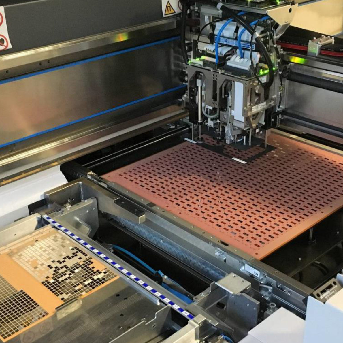
The embedding techniques we use combine the advantages of conventional PCB manufacturing with high-precision SMT component mounting. Component assembly can be divided into two main ap-proaches: “Face down” – the chip is mounted with the bond pads facing downwards – similarly to flip chips – and “face up” – the semiconductor is mounted with the bond pads facing upwards, as in wire bonding assembly. The resulting package is similar, but the two techniques lend themselves to different applications. The “face-down” approach is already popular in series manufacturing and is particularly suited to com-ponents with small pitch. The “face-up” technique is particularly suited to the embedding of vertical components, such as power MOSFETs, IGBTs and diodes.
Key research areas at Fraunhofer IZM include developing novel techniques for embedding electronic components in PCBs, investigating new basic and packaging materials and developing new processes for manufacturing HDI substrates.
 Fraunhofer Institute for Reliability and Microintegration IZM