Online-Session / February 13, 2024, 16:00 - 16:45 CET
Wafer-level Process Technologies for SiC/GaN Power Electronics
2# session of series »Powering the Future - Innovative Technologies for Power Electronics Modules with SiC and GaN Semiconductors«
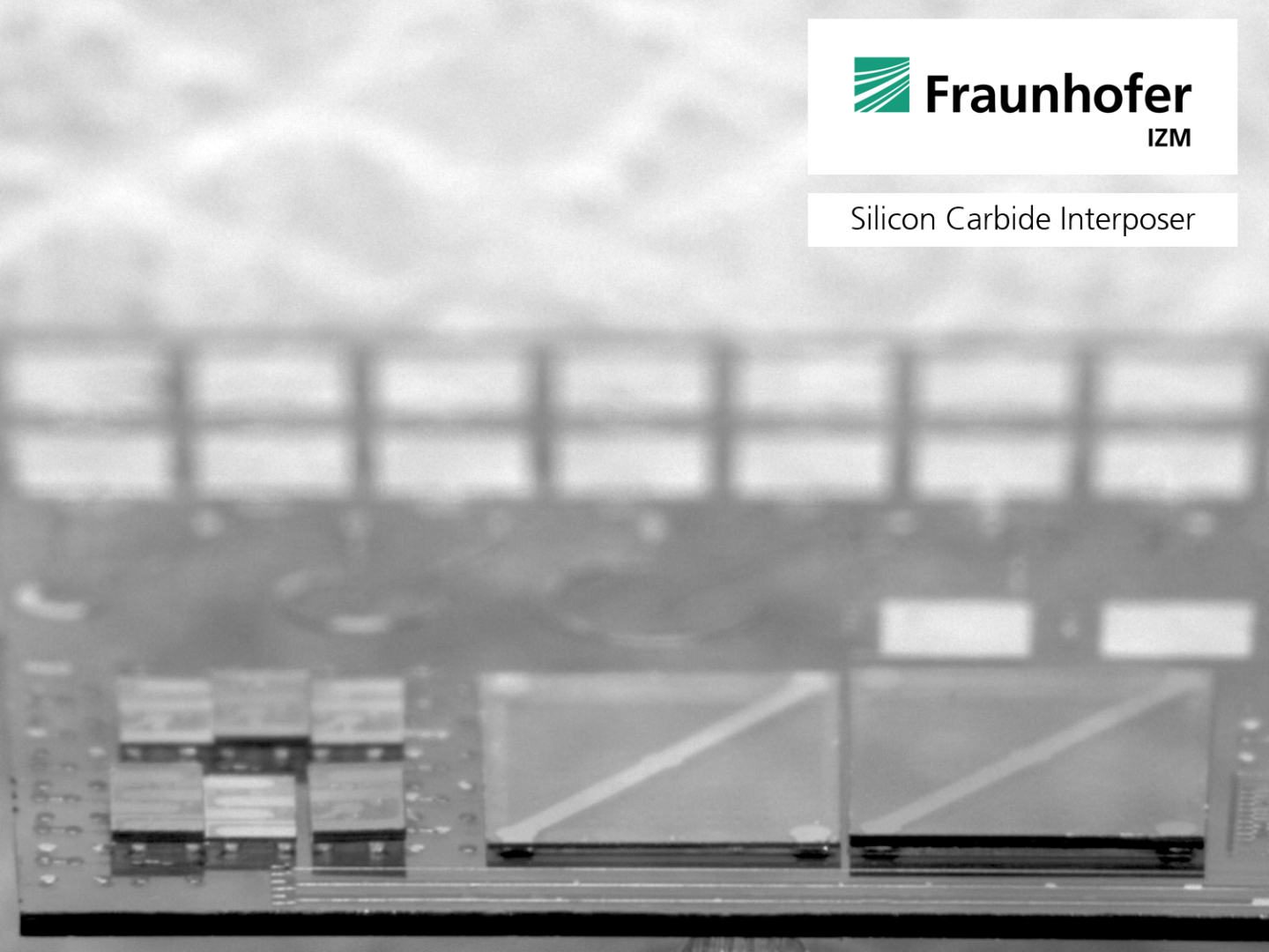
Silicon carbide attracted great attention in the past. Beside superior SiC electrical properties, best suitable for converters used in electrical vehicles and for power conversion, it also shows great mechanical and especially thermal properties which make this material very attractive as a possible packaging material. Its thermal conductivity, which is between 350 W/mK (4H SiC) and 500 W/mK (6H SiC), is superior to other materials used for Fan-out wafer level packaging (FOWLP) application like EMC with around 0.7 W/mK. The thermal concept of the electronic package for high power devices needs to address the increased temperature of operation and the need to ensure the heat dissipation of the device. In common Fan-out packages, Epoxy Mold Compounds (EMC) are used which does not handle high temperature operations well since EMC has a low thermal conductivity.
This session covers wafer level packaging techniques making use of SiC. A manufacturing process for a SiC Fan-out wafer level package will be presented. This package consists of two SiC wafers (a SiC frame wafer and a SiC head spreader wafer) that are processed separately and bonded together in further step. Also, the high-power chip is embedded to form a package.
An approach of 3D integration making use of Though Silicon Carbide Vias (TSiCV) - similar to the well-established TSV process – is demonstrated in this session as well.
 Fraunhofer Institute for Reliability and Microintegration IZM
