Communication Module Development

image - Glaswafer mit planaren Teststrukturen für Materialcharakterisierung
Glass wafer with planar test structures for characterizing materials
Ein Paar von Split-Ring Resonatoren gekoppelt an eine Coplanar-Leitung
© Fraunhofer IZM
A pair of split-ring resonators, connected to a co-planar line

The Communication Module Development Group explores how materials interact with high-frequency waves, including established packaging materials like conventional circuit boards and extending to other materials not primarily meant for packaging, but used in the automotive or communication sectors. The real-world uses of these materials range from low-frequency wireless data transmission (e.g. WLAN or Bluetooth) to 5G and 6G communication, satellite communication, and automotive radar systems.

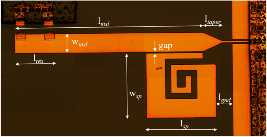
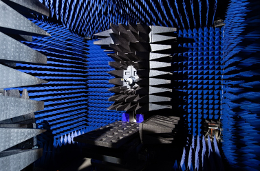
Our group continues to research and refine measuring techniques and methods for one of our focus areas: Determining the permittivity and dielectric loss tangent of different materials up to the THz range.

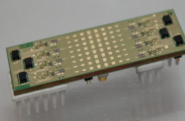
Beyond our commitment to refining the means and processes for materials characterization in the highest frequency ranges, we are exploring the impact of aging on dielectic properties in our quest to understand how the behaviour of systems as they age. These insights help find the design parameters for longer-lasting components and thereby contribute to more eco-friendly designs for electronic systems.

We are also testing novel meta-material concepts for use in HF system integration.

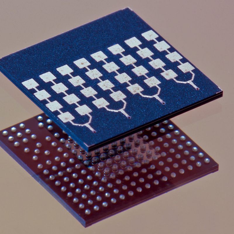
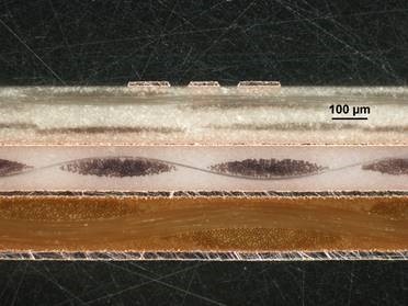
Our work covers a range of materials, including circuit boards, different synthetic materials (e.g. for mold or underfill uses, adhesives, or polymers in general), glass, ceramic, and others.

Packaging for high-frequency integrated circuits

Aufbau- und Verbindungstechnik für die Hochfrequenzsysteme / High-frequency packaging
© Fraunhofer IZM

Packaging of communication modules comprises a multitude of technologies. Due to rising operation frequencies the impact of interconnects to signal amplitude and integrity becomes more relevant. We develop, analyze and optimize package designs close to all technologies.

more info

Antenna in package development

Antennas are core components in wireless communication and radar systems. Due to the increasing operating frequencies (millimeter-Waves and sub-THz frequencies), integrated antennas in particular are becoming more and more relevant for so-called antenna-in-package (AiP) modules. AiP modules allow for an integration of all passive and active components in one platform.

more info

6G packaging

The manufacturing processes for cost-effective antenna packages for 6G applications have already been demonstrated successfully.
© Fraunhofer IZM

While the microelectronic market is more and more shifting to 5G and mmWave 5G, the research community is already working on the 6th generation of mobile communication. Forecasts see decisive advantages in using frequencies in the sub-THz frequency range. The D-band (110 - 170 GHz) in particular is therefore intensively investigated.

more info

New methods for materials characterization

Hochfrequenz- Charakterisierung, Design & Optimierung von Packaging-Technologien und Interconnects
© Fraunhofer IZM | Volker Mai

The ongoing miniaturization and advancement of high-frequency electronics poses new challenges to the materials applied in the systems. The issue is particularly evident in dielectric materials, which include substrate materials such as laminates or ceramics, epoxy mold compounds, underfillers, RDL polymers and many more.

more info

With reflect arrays and reflective surfaces towards energy efficient communication networks

The biggest technical challenge in implementing 6G is to cope with the elevated free-space attenuation. One solution that is being discussed as a disruptive technology in the radio frequency research community is Reconfigurable Intelligent Surfaces (RIS). RIS function as adjustable reflectors for high-frequency radiation.

more info

High-Q package integrated resonators

Package-integrierte Resonatoren mit hoher Güte
© Fraunhofer IZM

Modern trends towards miniaturization and the demand for higher resolution are driving radar technologies to explore and use frequencies at around 75-110 GHz. A planar spiral resonator operating at 13 GHz was developed at Fraunhofer IZM which followed by frequency multiplier is intended to serve for VCO operating at W-band.

more info

Cross-section of a metal planar resonator
Offener Resonator
© Fraunhofer IZM | Volker Mai
Open resonator for characterizing non-metal samples at up to 140 GHz
  • Measuring the dielectic properties (permittivity and loss factor) of different materials
  • Modelling, designing, laying out, and measuring planar resonators for characterizing metallized substrates
  • Characterizing materials across different temperature ranges
  • Determining the impact of humidity absorption on dielectric properties
  • Accelerated aging of materials
  • Advising on the selection of dielectric materials suited to the chosen application

High-frequency design, measurement and optimization of packaging interconnects from 100 MHz to 500 GHz

Hochfrequenz- Charakterisierung, Design & Optimierung von Packaging-Technologien und Interconnects
© Fraunhofer IZM | Volker Mai
  • Chip interconnections, e.g., bond wires, ribbon bonds and flip-chip interconnects
  • Planar and vertical interconnects (e.g. transmission lines and vias) in redistribution layers, interposers/chip carriers (e.g., organic, mold, ceramic, glass and silicon), advanced packages (e.g., PCB embedding, fan out wafer level packaging) and in system-boards
  • Package-to-board and board-to-board interconnects (e.g., BGA balls, sinter interconnects)
  • RF connectors

Design, test and optimization of integrated antenna arrays and RF frontend components such as filters, power dividers and inductors for the following:

  • Wireless communication infrastructure (e.g., base stations) for 4G, 5G and future 6G mobile networks (radio access network, backhaul, core…)
  • Satellite communication systems for LEO, GEO and MEO (ground and space segments)
  • Radar sensors for automotive/autonomous driving, transportation systems (e.g., trains) and home automation

  • Measurement of radiation pattern and gain of antennas up to 325 GHz
  • Measurement of S-parameters of packaging interconnects, antennas and RF frontend components in dependency of frequency (up to 500 GHz) and temperature (-30°C to 150°C)
  • DIRECT CONTACT

  • Development of hardware architectures for wireless communication frontend modules, e.g. active antenna systems (AAS), multiple-input multiple-output (MIMO) antenna arrays-based modules, Antenna-in-Package (AiP) and Antenna-on-Package (AoP) solutions, Package-on-Package (PoP) configurations
  • Development of system integration platforms tailored to given application using a wide range of packaging technologies and considering RF, fabrication, thermal and thermo-mechanical reliability requirements
  • 3D electromagnetic field simulation of integration platforms and their packaging building blocks
  • RF, signal and power integrity compliant design and layout of frontend modules, also with regard to miniaturization and high density integration (HDI)
  • Measurement-based characterization of frontend modules and their building blocks

Selected projects

© Fraunhofer IZM
Test structures for the electrical characterization of substrates, in-ductors, and mounting / intercon-nects at up to 110 GHz

Advanced system engineering lab

High-Frequency Technology - Equipment and Tools - Advanced System Engineering Lab - Fraunhofer IZM - R3S
© Fraunhofer IZM

High-Frequency Technology - equipment and tools

The HF lab specializes in measuring planar, “on-wafer” test samples at up to 110 GHz and the 3D characterization of antenna modules in shielding cabins. We can also determine the dielectric parameters of substrates nondestructively.

more info


Video

Online expert Session: materials for RF applications: Quo vadis?

Dr. rer. nat. Julia-Marie Köszegi


Download

Flyer