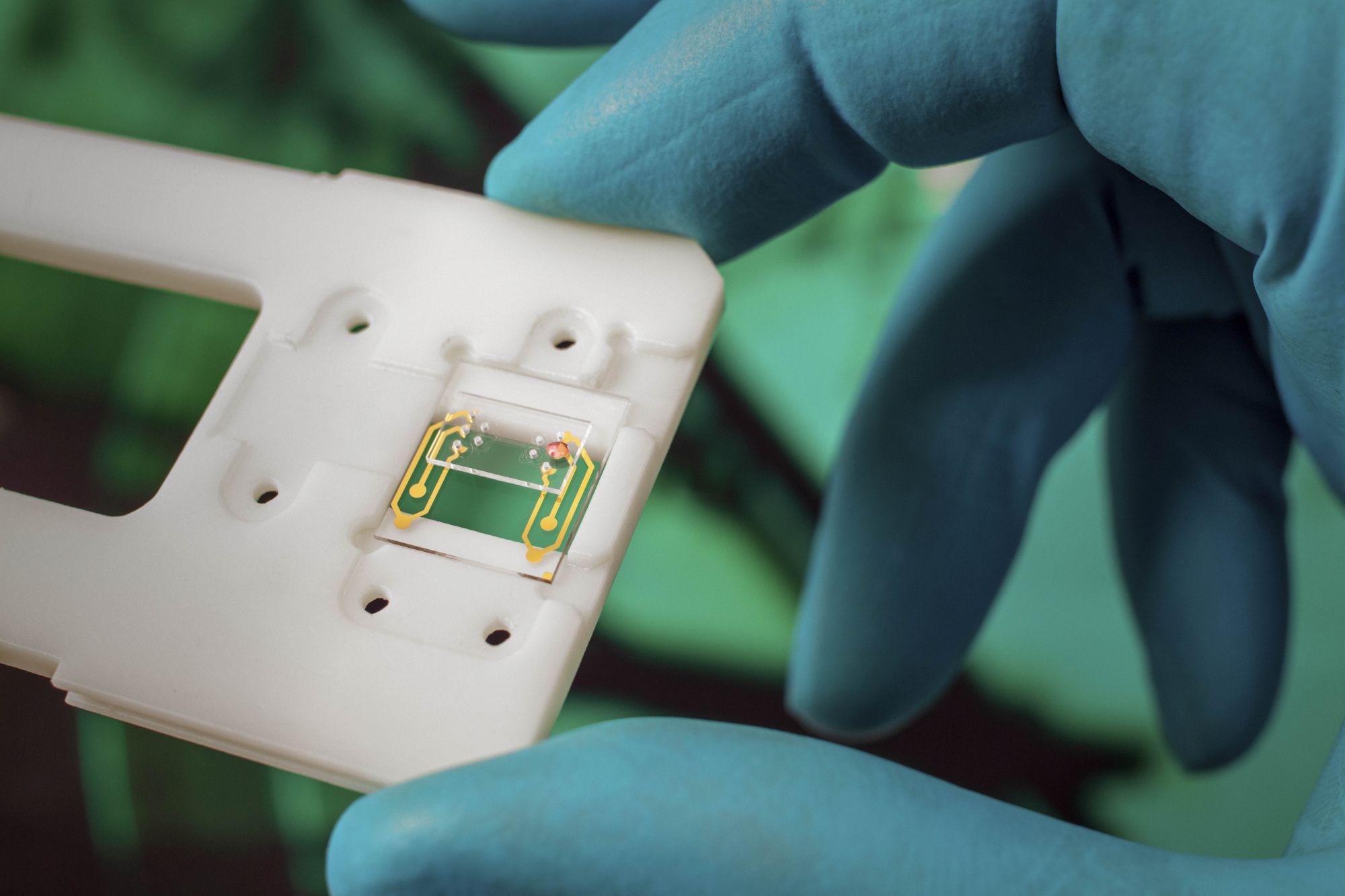

Complex and expensive bonding methods for planar optofluidic and electronic microsystems can be avoided by employing thin laser-structured doubled-sided tapes. They offer bonding solutions at room temperature to mainly integrate planar chips with mismatched thermal expansion coefficients. Microscale shapes can also be transferred to thin adhesive tapes using pulsed laser irradiation. This also opens up a new field of possibilities for simplifying the fabrication of microfluidic devices.
Fraunhofer IZM uses an automated laser system and a sub-micron precision bonding machine to develop application-specific solutions based on structured tapes. In particular, adhesive layers of the tapes in the thickness range of 35 – 80 µm have been investigated to produce tape-bonded optofluidic chips for Point-of-Care diagnostics. Small channels can be written directly with the pulsed laser beam, achieving smooth and straight edges. Tapes present unique features, high pressure-sensitivity and high adhesion, being excellent bonding layers between two different materials.
A variety of applications can be addressed such as healthcare, drug delivery, flexible microelectronics and among others under market-oriented R&D services and feasibility studies.
 Fraunhofer Institute for Reliability and Microintegration IZM