Electro-optical Circuit Board (EOCB)

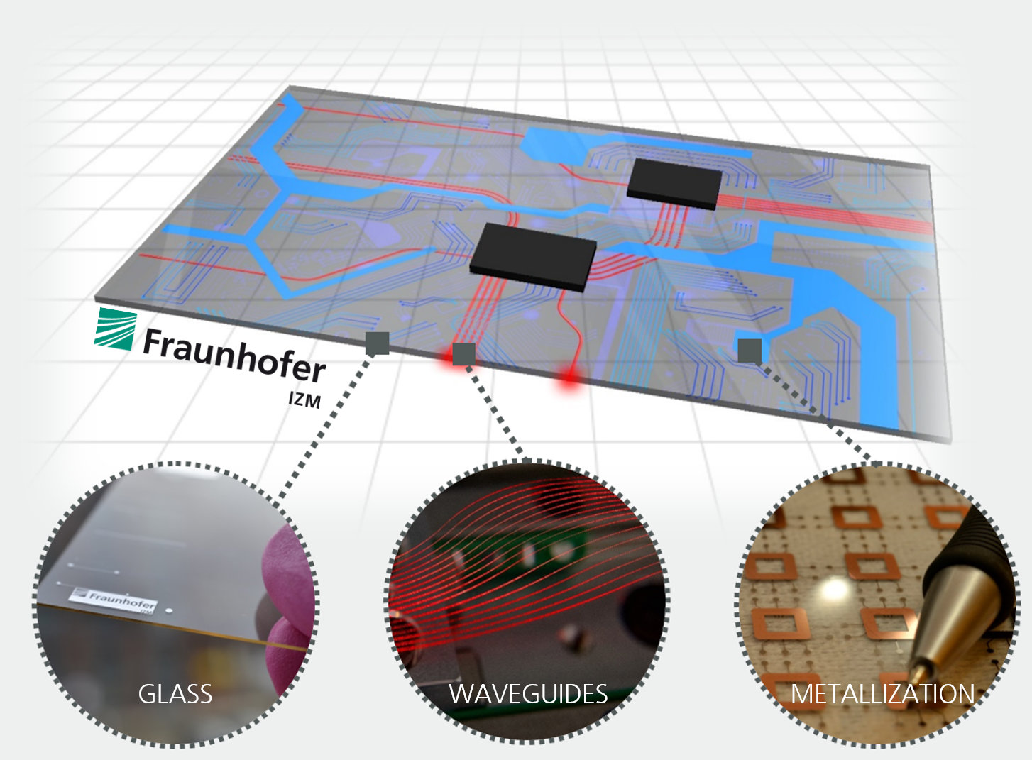
image - Electro-optical Circuit Board (EOCB)
© Fraunhofer IZM
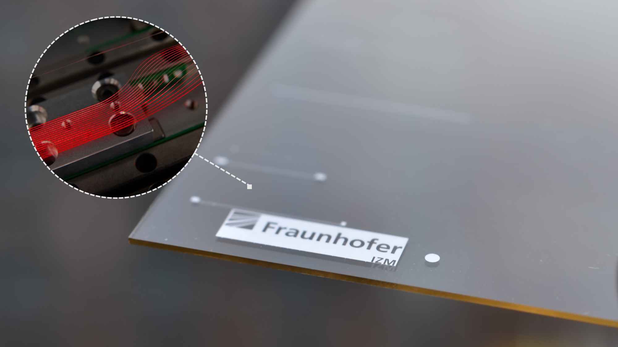
Illuminierte Lichtwellenleiter
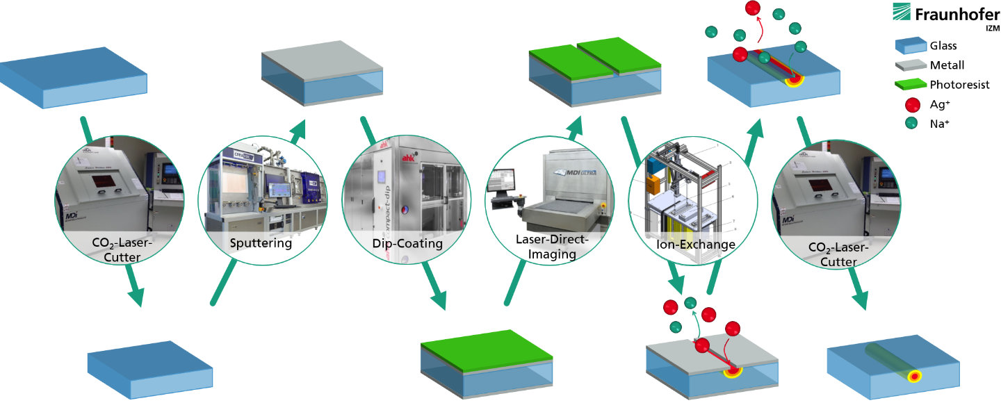
image - Process chain for integrating optical fibers into large-format thin glass.
© Fraunhofer IZM
Manufacturing process for optical fibers integrated in glass
  1. Modern telecommunications needs fast progress in photonic interconnection technology to keep pace with the massive growth of data being transmitted. The effects need to be felt in particular in the data centers that act as the interjections – and often bottlenecks – of this busy traffic system. But even in the field, enormous amounts of data need to be processed and transmitted, e.g. in self-driving cars.
  2. Many areas of research depend on optical sensor technology, typically using either free beams or fiber-routed light. Both choices, however, suffer from reliability and mechanical stability issues and often only offer low integration density.
  3. Quantum technology demands that the materials used in many applications need to be far more dimensionally stable and across a far wider temperature range than ever before, that the packaging is hermetically sealed, and that high transparency can be guaranteed across a broad spectrum of wavelengths.

The Solution

Combining electrical and optical layers in a single circuit board or chip can be a solution to all of these challenges. Fraunhofer IZM produced a first concept of such a combined electro-optical circuit board already in 1999 and has continued to make progress in the field. Since 2003, the necessary optical layer can be produced with commercially available large-format thin glass panels.

Electro-optical circuit boards or EOCB can realize the immense potential of optical signal transmissions for circuit board and chip design. In telecommunications, the waveguides included in the optical layer can receive the signals from fiber conductors and navigate them to their destinations on the circuit board. This combination of electrical and optical layers is currently receiving considerable attention in concepts like co-packaging. In optical sensor technology, waveguides of this type that let light interact specifically with the analytical targets promise a new level of versatility, as do the excellent properties of glass in terms of biocompatibility or chemical reactivity. Integration into thin glass panels offers better mechanical stability when compared to conventional fibers, and it circumvents the need for complex beamforming or guiding structures to allow for more densely packed designs. In quantum technology applications, a combination of electrical and optical functionality in glass also opens up new avenues for moving optical structures onto the system level.

In the past twenty years, Fraunhofer IZM has cooperated closely with research and industry partners to develop a process that can produce electro-optical circuit boards with commercial equipment at the following specifications:

  • Board formats up to 18” x 12”
  • Board thickness 300 to 700µm
  • optical layer
    • Graded index waveguides
    • Mono and multimodal
    • Propagation loss <0.6 dB/cm (@1550nm)
    • transparent at 400 to 1600 nm
  • electrical layer
    • structured metalization layers: Al, Cr, Cu, Ti, WTi
    • line space: up to 3µm
    • galvanization: Ag, Au, Cu, Ni
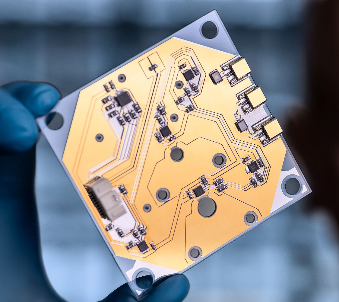
image LIDAR
© Fraunhofer IZM | Volker Mai
Elektrisch funktionalisiertes Glasboard für eine LIDAR Anwendung

Privacy warning

With the click on the play button an external video from www.youtube.com is loaded and started. Your data is possible transferred and stored to third party. Do not start the video if you disagree. Find more about the youtube privacy statement under the following link: https://policies.google.com/privacy

GISC

Pre-Development of an Optical Vertical Coupling Mechanism for the Passive and Automatable Interconnection of Photonic Components.

Isabella

Hybrid-Integrated and Frequency-Stabilized Lasers for the Reliable Manipulation of Ultracold Atoms for Transportable Systems

Troop

Developing a highly transparent dry film resist system ready for UV-A/VIS exposure (λ=350-450 nm) and UV structuring with variable layer thicknesses for the production of optical components

EPho

For the “Integrated Electro-Photonic Panel Systems” research project, Fraunhofer IZM has joined forces with the circuit board experts at ILFA, the glass refiners at Schröder Spezialglas, and the specialist tool engineers of FiconTec to create a new generation of high-speed circuit boards.


Download

Electro-optical Circuit Board

Selected Publications

2020

Schwietering, J.; Herbst, C.; Kirsch, O.; Arndt-Staufenbiel, N.; Wachholz, P.; Schröder, H.; Schneider-Ramelow, M.: Integrated optical single-mode waveguide structures in thin glass for flip-chip PIC assembly and fiber coupling. https://doi.org/10.1109/ECTC32862.2020.00036

2019

Schröder, H.; Neitz, M.; Schneider-Ramelow, M.: Demonstration of glass based photonic interposer for mid-board-optical engines and electro-optical circuit board (EOCB) integration strategy. https://doi.org/10.1117/12.2297363

Neitz, M.; Röder-Ali, J.; Marx, S.; Herbst, C.; Frey, C.; Schröder, H.; Lang, K.-D.: Insertion Loss Study for Panel-Level Single-Mode Glass Waveguides. https://doi.org/10.1117/12.2252802

2016

Brusberg, L.; Neitz, M.; Pernthaler, D.; Weber, D.; Sirbu, B.; Herbst, C.; Frey, C.; Queisser, M.; Wöhrmann, M.; Manessis, D.; Schild; B.; Oppermann, H.; Eichhammer, Y.; Schröder, H.; Håkansson, A.; Tekin, T.: Electro-optical circuit board with single-mode glass waveguide optical interconnects. https://doi.org/10.1117/12.2208103

Brusberg, L.; Whalley, S.; Pitwon, R.; Faridi, F.; Schröder, H.: Large Optical Backplane With Embedded Graded-Index Glass Waveguides and Fiber-Flex Termination.  https://doi.org/10.1109/JLT.2016.2529651

2003

Schröder, Henning; Arndt-Staufenbiel, Norbert; Cygon, Manfred; Scheel, Wolfgang (2003 pp. 1053-1059.): Planar Glass Waveguides for High Performance Electrical-Optical-Circuit-Boards (EOCB) - The Glass-Layer-Concept. The Glass-Layer-Concept. 53rd Electronic Components and Technology Conference. 53rd Electronic Components and Technology Conference, 2003. Proceedings., New Orleans, Louisiana, USA, 2003 pp. 1053-1059.

1999

Krabe, Detlef; Scheel, Wolfgang (Hg.) (1999): Optical interconnects by hot embossing for module and PCB technology - the EOCB approach. 49th Electronic Components and Technology Conference. San Diegeo, California, June 1-4.  10.1109/ECTC.1999.776342

This might also be of interest to you


News

Optical atomic clocks with record precision

Atomic clocks guarantee unrivalled precision when it comes to tracking time. They help us keep our digital and analogue clocks running on time by measuring the atomic resonance in cesium atoms exposed to microwave radiation. A new generation of optical atomic clocks is now set to increase their precision by a factor of up to 100,000.


REALIZM Blog

Will the printed circuit board of the future be made of glass?

High speed with optical signals

Newsletter

Stay in contact!

Get informed by email about technical news and events