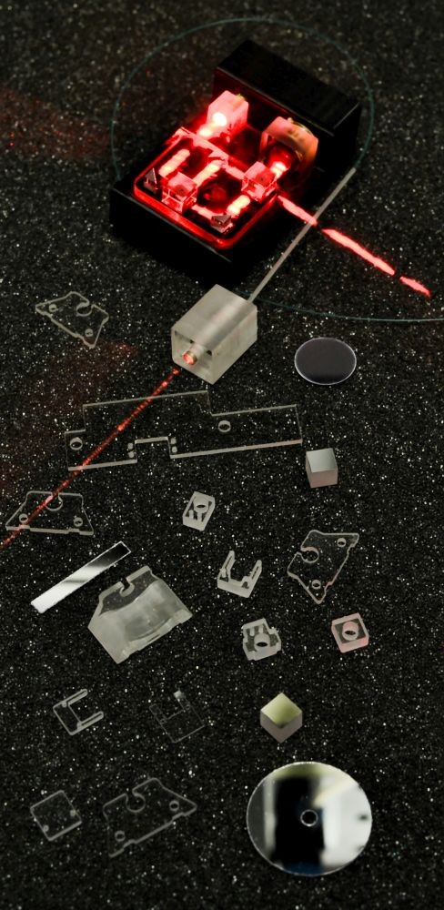
At the Fraunhofer IZM glass can be processed in a contactless manner using industrial, laser-assisted systems. Our solutions ensure precise and reproducible processing of glass for research and real-world applications. Depending on the specific application, the processes described below can be combined with each other in various ways.
Services
Selective Laser-Induced Etching (SLE)
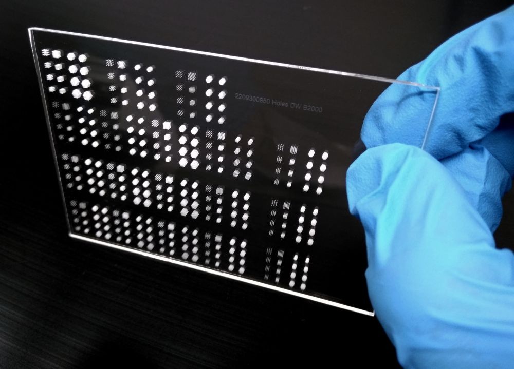
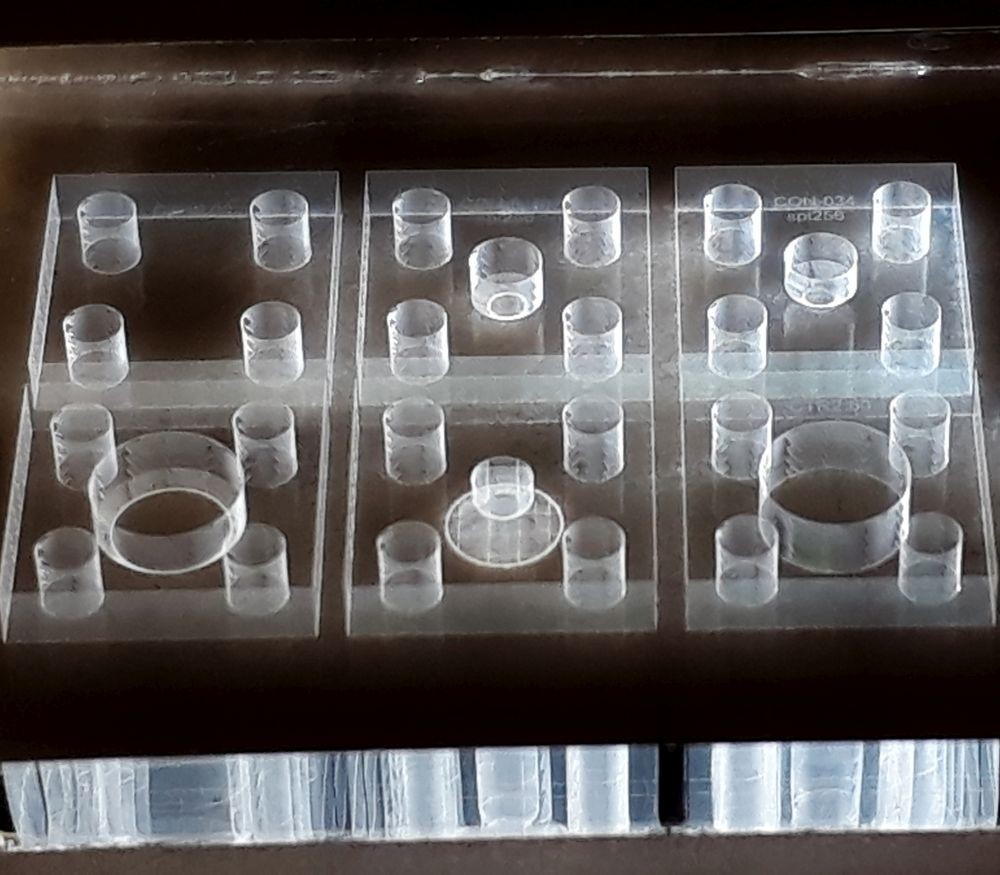
SLE is a two-step process creating advanced 3D microstructured glass wafers, panels or pieces. First, the glass is modified by ultra-short pulse laser radiation. Second, the modified material is removed by wet chemical etching. The selectivity of the etch is relevant for setting parameters, e.g. process speed and resolution, of the resulting structures. A large variety of geometries can be produced, like optical coupling structures, mechanical mounts, TGVs and fluidic microchannels for applications ranging from data communication & biomedicine to quantum technologies.
Features:
- Various 3D shapes (square, circular, irregular)
- Substrate size up to 200 x 200 mm (wafer or panel format)
- Substrate thickness from 0.1 mm to 6 mm
- Hole diameter from 20 µm (straight, tapered, shaped)
- Precision around ±1 μm possible
- Processed surface roughness Ra around 1 µm possible
- No micro cracks or chipping
- Many glass types (fused silica, borosilicate, aluminosilicate, sapphire)

Commercial SLE system: LightFab 3D Printer M
Direct laser structuring

Automated laser structuring and cutting machine: MDI LD600-H
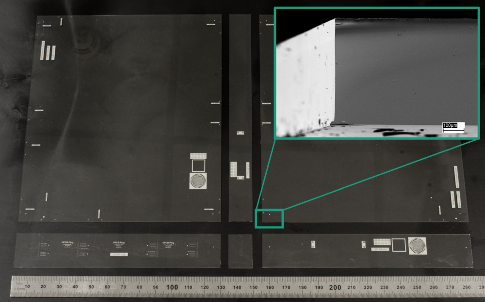
A short pulse laser (532 nm) enables processes such as drilling, free shape structuring, marking, engraving and stripping (removal of coatings/metallizations such as Cr, Al, Cu, ...) of glass. Due to the removal in layers, a limited three-dimensional structuring is also possible, e.g. for channels and cavities. The processing is freely programmable layout-based, no masks or similar are necessary.
Features:
- Various 2D and 2.5D shapes (square, circular, irregular)
- Substrate size up to 610 x 610 mm
- Substrate thickness from 0.1 mm to 8 mm
- Hole diameter from 150 µm (straight, tapered)
- Precision around ±10 μm possible
- Processed surface roughness around 2.5 µm possible
- Chipping <100 µm
- Many glass types (fused silica, borosilicate, aluminosilicate, soda lime)
Laser cutting
A CO2-laser (10600 nm) is used for stress-induced separation of glass. The laser beam heats the glass locally, followed by a controlled cooling. The induced mechanical stress leads to a precise crack formation in the glass during the subsequent breaking. The result is a clean and high-quality cut with highest edge strength (break resistance), since no microcracks or chipping occur. Furthermore, there is no material loss. The high glass edge quality allows direct optical coupling. Moreover, this method is distinguished by high cutting speeds and the elimination of further processing steps, e.g. grinding or polishing.
Features:
- Straight cutting (0° and 90°)
- Substrate size up to 610 x 610 mm
- Substrate thickness from 0.3 mm to 1 mm
- Cut position accuracy ±25 μm
- Optical, crack- and scratch-free glass edge quality without glass particles
- Many glass types (borosilicate, aluminosilicate, soda lime)